SLOS217I July 1998 – December 2024 THS3001
PRODUCTION DATA
- 1
- 1 Features
- 2 Applications
- 3 Description
- 4 Pin Configuration and Functions
- 5 Specifications
- 6 Detailed Description
- 7 Application and Implementation
- 8 Device and Documentation Support
- 9 Revision History
- 10Mechanical, Packaging, and Orderable Information
7.1.3 Slew Rate
The slew rate performance of a current-feedback amplifier, like the THS3001, is affected by many different factors. Some of these factors are external to the device, such as amplifier configuration and PCB parasitics, and others are internal to the device, such as available currents and node capacitance. Understanding some of these factors can help the PCB designer arrive at a more optimum circuit with fewer problems.
Whether the THS3001 is used in an inverting amplifier configuration or a noninverting configuration can impact the output slew rate. As can be seen from the specification tables as well as some of the figures in this data sheet, slew-rate performance in the inverting configuration is faster than in the noninverting configuration. This is because in the inverting configuration the input terminals of the amplifier are at a virtual ground and do not significantly change voltage as the input changes. Consequently, the time to charge any capacitance on these input nodes is less than for the noninverting configuration, where the input nodes actually do change in voltage an amount equal to the size of the input step. In addition, any PCB parasitic capacitance on the input nodes degrades the slew rate further simply because there is more capacitance to charge. Also, if the supply voltage (VCC) to the amplifier is reduced, slew rate decreases because there is less current available within the amplifier to charge the capacitance on the input nodes as well as other internal nodes.
Internally, the THS3001 has other factors that
impact the slew rate. The amplifiers behavior during the slew-rate transition varies
slightly depending upon the rise time of the input. This is because of the way the
input stage handles faster and faster input edges. Slew rates (as measured at the
amplifier output) of less than about
1500V/μs are
processed by the input stage in a linear fashion. Consequently, the output waveform
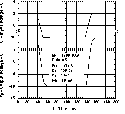
smoothly transitions between initial and final voltage levels. This is shown in
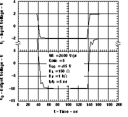
Figure 7-2. For slew rates greater than 1500V/μs, additional slew-enhancing transistors
present in the input stage begin to turn on to support these faster signals. The
result is an amplifier with extremely fast slew-rate capabilities. Figure 7-2 and Figure 7-3 show waveforms for these faster slew rates. The additional aberrations present in
the output waveform with these faster-slewing input signals are due to the brief
saturation of the internal current mirrors. This phenomenon, which typically lasts
less than 20ns, is considered normal operation and is not detrimental to the device
in any way. If for any reason this type of response is not desired, then increasing
the feedback resistor or slowing down the input-signal slew rate reduces the
effect.
 Figure 7-2 Slew Rate
 Figure 7-3 Slew Rate