SLOS217I July   1998  – December 2024 THS3001

PRODUCTION DATA  

  1.   1
  2. Features
  3. Applications
  4. Description
  5. Pin Configuration and Functions
  6. Specifications
    1. 5.1 Absolute Maximum Ratings
    2. 5.2 ESD Ratings
    3. 5.3 Recommended Operating Conditions
    4. 5.4 Thermal Information
    5. 5.5 Electrical Characteristics
    6. 5.6 Typical Characteristics
  7. Detailed Description
    1. 6.1 Overview
    2. 6.2 Functional Block Diagram
    3. 6.3 Device Functional Modes
  8. Application and Implementation
    1. 7.1 Application Information
      1. 7.1.1 Recommended Feedback and Gain Resistor Values
      2. 7.1.2 Noise Calculations
      3. 7.1.3 Slew Rate
      4. 7.1.4 Offset Voltage
    2. 7.2 Typical Applications
      1. 7.2.1 General Configurations
      2. 7.2.2 Driving a Capacitive Load
    3. 7.3 Power Supply Recommendations
    4. 7.4 Layout
      1. 7.4.1 Layout Guidelines
        1. 7.4.1.1 PCB Design Considerations
        2. 7.4.1.2 Thermal Considerations
  9. Device and Documentation Support
    1. 8.1 Device Support
      1. 8.1.1 Evaluation Board
    2. 8.2 Receiving Notification of Documentation Updates
    3. 8.3 Support Resources
    4. 8.4 Trademarks
    5. 8.5 Electrostatic Discharge Caution
    6. 8.6 Glossary
  10. Revision History
  11. 10Mechanical, Packaging, and Orderable Information

Evaluation Board

An evaluation board is available for the THS3001 (THS3001EVM). The board has been configured for low parasitic capacitance to optimize for the full performance of the amplifier. A schematic of the evaluation board is shown in Figure 8-1. The circuitry has been designed so that the amplifier can be used in either an inverting or noninverting configuration. For more detailed information, see the THS3001 EVM User's Guide. Order the evaluation board online through the TI web site, or through your local TI sales office or distributor.
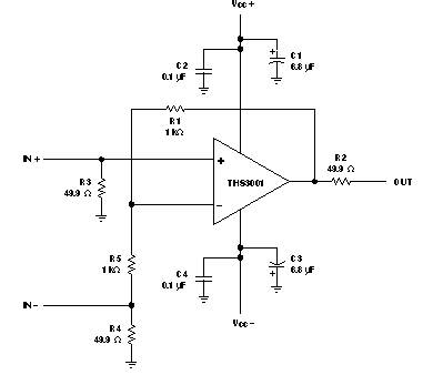
THS3001 THS3001 Evaluation Board
                    Schematic Figure 8-1 THS3001 Evaluation Board Schematic