TLV320AIC3107 Low-Power Stereo Codec With Integrated Mono Class-D Speaker Amplifier
1 Features
- Stereo CODEC With Integrated Mono Class-D Amplifier
- High Performance Audio DAC
- 97-dBA Signal-to-Noise Ratio (Single Ended)
- 16/20/24/32-Bit Data
- Supports Sample Rates From 8 kHz to 96 kHz
- 3D/Bass/Treble/EQ/De-Emphasis Effects
- Flexible Power Saving Modes and Performance are Available
- High Performance Audio ADC
- 92-dBA Signal-to-Noise Ratio
- Supports Rates From 8 kHz to 96 kHz
- Digital Signal Processing and Noise Filtering Available During Record
- Seven Audio Input Pins
- Programmable as 6 Single-Ended or 3 Fully Differential Inputs
- Capability for Floating Input Configurations
- Multiple Audio Output Drivers
- Mono Fully Differential or Stereo Single-Ended Headphone Drivers
- Single-Ended Stereo Line Outputs
- Mono 1 W Class-D BTL 8Ω Speaker Driver
- Low Power Consumption: 15-mW Stereo 48-kHz Playback With 3.3-V Analog Supply
- Ultra-Low Power Mode with Passive Analog Bypass
- Programmable Input/Output Analog Gains
- Automatic Gain Control (AGC) for Record
- Programmable Microphone Bias Level
- Programmable PLL for Flexible Clock Generation
- I2C™ Control Bus
- Audio Serial Data Bus Supports I2S, Left/Right-Justified, DSP, and TDM Modes
- Extensive Modular Power Control
- Power Supplies:
- Speaker Amp: 2.7 V – 5.5 V
- Analog: 2.7 V – 3.6 V.
- Digital Core: 1.525 V – 1.95 V
- Digital I/O: 1.1 V – 3.6 V
- Packages: 5-mm × 5-mm 40-QFN, 0.4-mm Pitch
3.563-mm × 3.376-mm 42-DSBGA, 0.5 mm Pitch
(Product Preview)
2 Applications
- Cellular Handsets
- Digital Cameras
- Portable Media Players
- General Portable Audio Equipment
3 Description
The TLV320AIC3107 is a low power stereo audio codec with stereo headphone amplifier, and mono class-D speaker driver, as well as multiple inputs and outputs programmable in single-ended or
fully differential configurations.
Device Information(1)
| PART NUMBER | PACKAGE | BODY SIZE (MAX) |
|---|---|---|
| TLV320AIC3107 | WQFN (40) | 5.15 mm × 5.15 mm |
| DSBGA (42) | 3.563 mm × 3.376 mm |
- For all available packages, see the orderable addendum at the end of the datasheet.
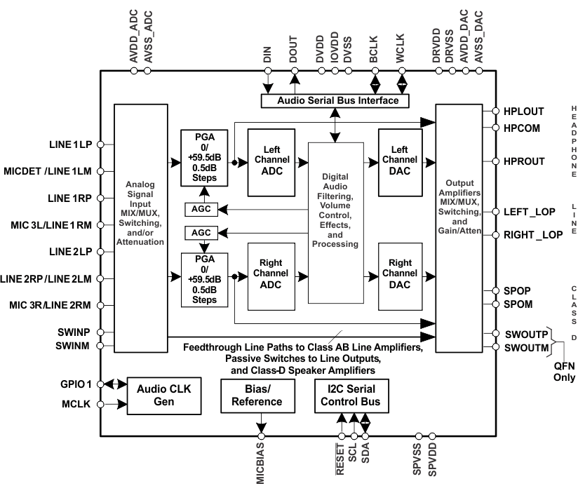
4 Simplified Block Diagram
5 Revision History
Changes from C Revision (March 2009) to D Revision
- Added Pin Configuration and Functions section, ESD Ratings table, Feature Description section, Device Functional Modes, Application and Implementation section, Power Supply Recommendations section, Layout section, Device and Documentation Support section, and Mechanical, Packaging, and Orderable Information section Go
6 Description (Continued)
Extensive register-based power control is included, enabling stereo 48-kHz DAC playback as low as 15 mW from a 3.3-V analog supply, making it ideal for portable battery-powered audio and telephony applications.
The high-power output drivers are capable of driving a variety of load configurations, including up to three channels of single-ended 16-Ω headphones using ac-coupling capacitors, or stereo 16-Ω headphones in a capacitorless output configuration. The mono class-D output is capable of differentially driving an 8-Ω speaker.
The stereo audio DAC supports sampling rates from 8 kHz to 96 kHz and includes programmable digital filtering in the DAC path for 3D, bass, treble, midrange effects, speaker equalization, and de-emphasis for 32-kHz, 44.1-kHz, and 48-kHz rates. The stereo audio ADC supports sampling rates from 8 kHz to 96 kHz and is preceded by programmable gain amplifiers or AGC that can provide up to 59.5 dB analog gain for low-level microphone inputs. The TLV320AIC3107 provides an extremely high range of programmability for both attack (8-1,408 ms) and for decay (0.05-22.4 seconds). This extended AGC range allows the AGC to be tuned for many types of applications.
For battery saving applications where neither analog nor digital signal processing are required, the device can be put in a special analog signal passthru mode. This mode significantly reduces power consumption, as most of the device is powered down during this pass through operation.
The serial control bus supports I2C protocol, while the serial audio data bus is programmable for I2S, left/right-justified, DSP, or TDM modes. A highly programmable PLL is included for flexible clock generation and support for all standard audio rates from a wide range of available MCLKs, varying from 512 kHz to 50 MHz, with special attention paid to the most popular cases of 12-MHz, 13-MHz, 16-MHz, 19.2-MHz, and 19.68-MHz system clocks.
The TLV320AIC3107 operates from an analog supply of 2.7 V–3.6 V, a digital core supply of 1.65 V–1.95 V, a digital I/O supply of 1.1 V–3.6 V, and a speaker amplifier supply of 2.7V–5.5V. The device is available in the 5 × 5-mm, 40-pin QFN package and in the future a 3.5 × 3-mm, 42-lead DSBGA package.
The record path of the TLV320AIC3107 contains integrated microphone bias, digitally controlled stereo microphone preamplifier, and automatic gain control (AGC), with mix/mux capability among the multiple analog inputs. Programmable filters are available during record which can remove audible noise that can occur during optical zooming in digital cameras. The playback path includes mix/mux capability from the stereo DAC and selected inputs, through programmable volume controls, to the various outputs.
The TLV320AIC3107 contains three high-power output drivers as well as two single-ended line output drivers, and a differential class-D output driver.
7 Pin Configuration and Functions


Pin Functions
| PIN | I/O | DESCRIPTION | ||
|---|---|---|---|---|
| QFN | WCSP(1) | NAME | ||
| 1 | A1 | SCL | I | I2C serial clock |
| 2 | B1 | SDA | I/O | I2C serial data input/output |
| 3 | A2 | MICDET/LINE1LM | I | MIC1 or Line1 analog input (left – or multifunctional) or Microphone detect |
| 4 | A3 | LINE1LP | I | MIC1 or Line1 analog input (left + or multifunctional) |
| 5 | B3 | LINE1RP | I | MIC1 or Line1 analog input (R + or multifunctional) |
| 6 | A4 | MIC3L/LINE1RM | I | MIC3 or Line1 analog input (R - or multifunctional) |
| 7 | B4 | LINE2LP | I | MIC2 or Line2 analog input (left + or multifunctional) |
| 8 | A5 | LINE2RP/LINE2LM | I | MIC2 or Line2 analog input (left + or right - or multifunctional) |
| 9 | A6 | MIC3R/LINE2RM | I | MIC3 or Line2 analog input (right + or multifunctional) |
| 10 | B5 | MICBIAS | O | Microphone bias voltage output |
| 11 | B6 | AVSS_ADC | G | ADC analog ground supply, 0 V |
| 12 | C4 | AVDD_ADC | P | ADC analog voltage supply, 2.7 V–3.6 V |
| 13 | C5 | DRVDD | P | High-power output driver analog voltage supply, 2.7 V–3.6 V |
| 14 | C6 | HPLOUT | O | High-power output driver (left +) |
| 15 | D5 | HPCOM | O | High-power output driver (left – or multifunctional) |
| 16 | D4 | DRVSS | G | High-power output driver analog ground supply, 0 V |
| 17 | D6 | HPROUT | O | High-power output driver (right +) |
| 18 | E5 | DRVDD | P | High-power output driver analog voltage supply, 2.7 V–3.6 V |
| 19 | E6 | LEFT_LOP | O | Left line output |
| 20 | F6 | RIGHT_LOP | O | Right line output |
| 21 | F5 | AVDD_DAC | P | DAC analog voltage supply, 2.7 V–3.6 V |
| 22 | G6 | AVSS_DAC | G | DAC analog ground supply, 0 V |
| 23 | F4 | SPOM | O | Class-D (or Bypass SW, WCSP only) negative differential output |
| 24 | F2, G1, G2, G3, G5 | SPVSS | G | Class-D ground supply, 0 V |
| 25 | G4 | SPVDD | P | Class-D voltage supply, 2.7 V–5.5 V |
| 26 | F3 | SPOP | O | Class-D (or Bypass SW, WCSP only) positive differential output |
| 27 | E4 | SWINM | I | Negative Bypass Switch Input |
| 28 | — | SWOUTM | O | Negative Bypass Switch Output, to be tied to SPOM externally |
| 29 | — | SWOUTP | O | Positive Bypass Switch Output, to be tied to SPOP externally |
| 30 | E3 | SWINP | I | Positive Bypass Switch Input |
| 31 | F1 | RESET | I | Reset |
| 32 | E2 | GPIO1 | I/O | General-purpose input/output |
| 33 | D3 | DVDD | P | Digital core voltage supply, 1.525 V–1.95 V |
| 34 | E1 | MCLK | I | Master clock input |
| 35 | D2 | BCLK | I/O | Audio serial data bus bit clock (input/output) |
| 36 | D1 | WCLK | I/O | Audio serial data bus word clock (input/output) |
| 37 | C2 | DIN | I | Audio serial data bus data input (input) |
| 38 | C1 | DOUT | O | Audio serial data bus data output (output) |
| 39 | C3 | DVSS | G | Digital core / I/O ground supply, 0 V |
| 40 | B2 | IOVDD | P | I/O voltage supply, 1.1 V–3.6 V |
8 Specifications
8.1 Absolute Maximum Ratings
over operating free-air temperature range (unless otherwise noted)(1)(2)| MIN | MAX | UNIT | ||
|---|---|---|---|---|
| AVDD_DAC to AVSS_DAC, DRVDD to DRVSS, AVSS_ADC | –0.3 | 3.9 | V | |
| SPVDD to SPVSS | –0.3 | 6.0 | V | |
| AVDD to DRVSS | –0.3 | 3.9 | V | |
| IOVDD to DVSS | –0.3 | 3.9 | V | |
| DVDD to DVSS | –0.3 | 2.5 | V | |
| AVDD_DAC to DRVDD | –0.1 | 0.1 | V | |
| Digital input voltage to DVSS | –0.3 | IOVDD + 0.3 | V | |
| Analog input voltage to AVSS_ADC | –0.3 | AVDD + 0.3 | V | |
| Operating temperature range | –40 | 85 | °C | |
| TJ Max | Junction temperature | 105 | °C | |
| Power dissipation | (TJ Max – TA)/θJA | |||
| Tstg | Storage temperature range | –65 | 105 | °C |
8.2 ESD Ratings
| VALUE | UNIT | |||
|---|---|---|---|---|
| V(ESD) | Electrostatic discharge | Human-body model (HBM), per ANSI/ESDA/JEDEC JS-001(1) | ±2300 | V |
| Charged-device model (CDM), per JEDEC specification JESD22-C101(2) | ±1000 | |||
8.3 Recommended Operating Conditions
over operating free-air temperature range (unless otherwise noted)| MIN | NOM | MAX | UNIT | ||
|---|---|---|---|---|---|
| AVDD_DAC, DRVDD(1) | Analog supply voltage | 2.7 | 3.3 | 3.6 | V |
| DVDD(1) | Digital core supply voltage | 1.525 | 1.8 | 1.95 | V |
| IOVDD(1) | Digital I/O supply voltage | 1.1 | 1.8 | 3.6 | V |
| SPVDD | Speaker Amplifier supply voltage | 2.7 | 3.6 | 5.5 | V |
| VI | Analog full-scale 0 dB input voltage (DRVDD1 = 3.3 V) (Single Ended) | 0.707 | VRMS | ||
| Stereo line output load resistance | 10 | kΩ | |||
| Stereo headphone output load resistance | 16 | Ω | |||
| Digital output load capacitance | 10 | pF | |||
| TA | Operating free-air temperature | –40 | 85 | °C | |
8.4 Thermal Information
| THERMAL METRIC(1) | TLV320AIC3107 | UNIT | ||
|---|---|---|---|---|
| RSB | YZF | |||
| 40 PINS | 42 PINS | |||
| RθJA | Junction-to-ambient thermal resistance | 30.7 | 49.5 | °C/W |
| RθJC(top) | Junction-to-case (top) thermal resistance | 16 | 0.1 | |
| RθJB | Junction-to-board thermal resistance | 4.6 | 7.1 | |
| ψJT | Junction-to-top characterization parameter | 0.2 | 0.8 | |
| ψJB | Junction-to-board characterization parameter | 4.5 | 7 | |
| RθJC(bot) | Junction-to-case (bottom) thermal resistance | 0.9 | n/a | |
8.5 Dissipation Ratings(1)
| PACKAGE TYPE | TA = 25°C POWER RATING |
DERATING FACTOR | TA = 75°C POWER RATING |
TA = 85°C POWER RATING |
|---|---|---|---|---|
| DSBGA(2) | 1.60 W | 20 mW/°C | 600 mW | 400 mW |
| QFN | 2.35 W | 29.4 mW/° C | 882 mW | 588 mW |
8.6 Electrical Characteristics
At 25°C, AVDD_DAC = 3.3 V, DRVDD = 3.3 V, SPVDD = 5 V, IOVDD = 3.3 V, DVDD = 1.8 V, Fs = 48-kHz, 16-bit audio data(unless otherwise noted)
| PARAMETER | TEST CONDITIONS | MIN | TYP | MAX | UNIT | ||
|---|---|---|---|---|---|---|---|
| AUDIO ADC | |||||||
| Input signal level (0 dB) | Single-ended input | 0.707 | VRMS | ||||
| Signal-to-noise ratio, A-weighted(1)(2) | Fs = 48 ksps, 0 dB PGA gain, Inputs ac-shorted to ground | 80 | 92 | dB | |||
| Dynamic range (2) | Fs = 48 ksps, 0 dB PGA gain, –60 dB full-scale input signal |
91 | dB | ||||
| THD | Total harmonic distortion | Fs = 48 ksps, 0 dB PGA gain, –2dB full-scale 1kHz input signal |
–88 | –70 | dB | ||
| Power supply rejection ratio | 217 Hz signal applied to DRVDD | 49 | dB | ||||
| 1 kHz signal applied to DRVDD | 46 | ||||||
| Gain error | Fs = 48 ksps, 0 dB PGA gain, –2dB full-scale 1kHz input signal |
0.84 | dB | ||||
| Input channel separation | 1 kHz, -2dB full-scale signal, MIC3L to MIC3R | -86 | dB | ||||
| 1 kHz, -2dB full-scale signal, MIC2L to MIC2R | -98 | ||||||
| 1 kHz, -2dB full-scale signal, MIC1L to MIC1R | -75 | ||||||
| ADC programmable gain amplifier maximum gain | 1-kHz input tone | 59.5 | dB | ||||
| ADC programmable gain amplifier step size | 0.5 | dB | |||||
| Input resistance | LINE1L inputs routed to single ADC Input mix attenuation = 0 dB |
20 | kΩ | ||||
| LINE1L inputs routed to single ADC, input mix attenuation = 12 dB |
80 | ||||||
| LINE2L inputs routed to single ADC Input mix attenuation = 0 dB |
20 | ||||||
| LINE2L inputs routed to single ADC, input mix attenuation = 12 dB |
80 | ||||||
| Input level control minimum attenuation setting | 0 | dB | |||||
| Input level control maximum attenuation setting | 12 | dB | |||||
| Input signal level | Differential Input | 1.414 | VRMS | ||||
| Signal-to-noise ratio, A-weighted(1)(2) | Fs = 48 ksps, 0 dB PGA gain, Inputs ac-shorted to ground, Differential Mode | 92 | dB | ||||
| THD | Total harmonic distortion | Fs = 48 ksps, 0 dB PGA gain, –2dB Full-scale 1kHz input signal, Differential Mode | –91 | dB | |||
| ANALOG PASS THROUGH MODE | |||||||
| Input to output switch resistance, (rDS(on)) | LINE1L to LEFT_LOP | 330 | Ω | ||||
| LINE1R to RIGHT_LOP | 330 | ||||||
| SWINP to SWOUTP | 1 | ||||||
| SWINM to SWOUTM | 1 | ||||||
| ADC DIGITAL DECIMATION FILTER, Fs = 48 kHz | |||||||
| Filter gain from 0 to 0.39 Fs | ±0.1 | dB | |||||
| Filter gain at 0.4125 Fs | –0.25 | dB | |||||
| Filter gain at 0.45 Fs | –3 | dB | |||||
| Filter gain at 0.5 Fs | –17.5 | dB | |||||
| Filter gain from 0.55 Fs to 64 Fs | –75 | dB | |||||
| Filter group delay | 17/Fs | s | |||||
| MICROPHONE BIAS | |||||||
| Bias voltage | Programmable setting = 2.0 | 2 | V | ||||
| Programmable setting = 2.5 | 2.3 | 2.5 | 2.7 | ||||
| Programmable setting = DRVDD | DRVDD | ||||||
| Current sourcing | Programmable setting = 2.5V | 4 | mA | ||||
| AUDIO DAC - SINGLE ENDED LINE OUTPUT, LOAD = 10 kΩ | |||||||
| Full-scale output voltage | 0 dB Input full-scale signal, output volume control = 0 dB, Output common mode setting = 1.35 V |
0.707 | Vrms | ||||
| Signal-to-noise ratio, A-weighted | No input signal, output volume control = 0 dB, Output common mode setting = 1.35 V, Fs = 48 kHz |
97 | dB | ||||
| Total harmonic distortion | 0 dB 1 kHz input full-scale signal, Output volume control = 0 dB, Output common mode setting = 1.35 V, Fs = 48 kHz |
-84 | -70 | dB | |||
| DAC Gain Error | 0 dB 1 kHz input full-scale signal, Output volume control = 0 dB, Output common mode setting = 1.35 V, Fs = 48 kHz |
-0.8 | dB | ||||
| AUDIO DAC - SINGLE ENDED HEADPHONE OUTPUT, LOAD = 16 Ω | |||||||
| Full-scale output voltage | 0 dB Input full-scale signal, Output volume control = 0 dB, Output common mode setting = 1.35 V |
0.707 | Vrms | ||||
| Signal-to-noise ratio, A-weighted | No input signal, output volume control = 0 dB, Output common mode setting = 1.35 V, Fs = 48 kHz |
95 | dB | ||||
| No input signal, output volume control = 0 dB, Output common mode setting = 1.35 V, Fs = 48 kHz, 50% DAC Current Boost Mode |
96 | dB | |||||
| Dynamic range, A-weighted | –60 dB 1 kHz input full-scale signal, Output volume control = 0 dB, Output common mode setting = 1.35 V, Fs = 48 kHz |
92 | dB | ||||
| Total harmonic distortion | 0 dB 1 kHz input full-scale signal, Output volume control = 0 dB, Output common mode setting = 1.35 V, Fs = 48 kHz |
-84 | -65 | dB | |||
| Power supply rejection ratio | 217 Hz Signal applied to DRVDD, AVDD_DAC | 41 | dB | ||||
| 1 kHz Signal applied to DRVDD, AVDD_DAC | 44 | ||||||
| DAC channel separation | 0 dB Full-scale input signal between left and right Lineout | 84 | dB | ||||
| DAC Gain Error | 0 dB 1 kHz input full-scale signal, Output volume control = 0 dB, Output common mode setting = 1.35 V, Fs = 48 kHz |
-1 | dB | ||||
| AUDIO DAC - LINEOUT AND HEADPHONE OUT DRIVERS | |||||||
| Output common mode | First option | 1.35 | V | ||||
| Second option | 1.5 | ||||||
| Third option | 1.65 | ||||||
| Fourth option | 1.8 | ||||||
| Output volume control max setting | 9 | dB | |||||
| Output volume control step size | 1 | dB | |||||
| SPEAKER AMPLIFIER OUTPUT, LOAD = 8 Ω | |||||||
| Full-scale output voltage | 1 kHz, 0dB full-scale input signal, Output volume control for left line output = 0 dB, for class-D = 0 dB Output common mode setting = 1.35 V, Fs = 48 kHz |
2.5 | Vrms | ||||
| Output voltage | 1 kHz, 0dB full-scale input signal, Output volume control for left line output = -4.5 dB, for class-D = 6 dB Output common mode setting = 1.35 V, Fs = 48 kHz |
2.875 | Vrms | ||||
| Idle Channel Noise | No input signal, output gain control = 0 dB | -92 | dB | ||||
| Dynamic range, A-weighted | 1 kHz,–60 dB full-scale input signal, Output volume control for left line output = 0 dB, for class-D = 0 dB Output common mode setting = 1.35 V, Fs = 48 kHz |
91 | dB | ||||
| Total harmonic distortion | 1 kHz, 0 dB full-scale input signal, Output volume control for left line output = –4.5 dB, for class-D = 6 dB Output common mode setting = 1.35 V, Fs = 48 kHz, 1 W output power |
1.77% -35 |
dB | ||||
| Total harmonic distortion | 1 kHz, –6 dB full-scale input signal, Output volume control for left line output = –4.5 dB, for class-D = 6 dB Output common mode setting = 1.35 V, Fs = 48 kHz, 250 mW output power |
0.056% -65 |
0.316% -50 |
dB | |||
| Power supply rejection ratio | 217 Hz Signal applied to SPVDD | 37 | dB | ||||
| 1 kHz Signal applied to SPVDD | 33 | ||||||
| Gain Error | 1 kHz, 0 dB input full-scale signal, Output volume control = 0 dB, Output common mode setting = 1.35 V, Fs = 48 kHz |
-1.6 | dB | ||||
| DAC DIGITAL INTERPOLATION – FILTER Fs = 48-ksps | |||||||
| Passband | 0 | 0.45 × Fs | Hz | ||||
| Passband ripple | ±0.06 | dB | |||||
| Transition band | 0.45 × Fs | 0.55 × Fs | Hz | ||||
| Stopband | 0.55 × Fs | 7.5 × Fs | Hz | ||||
| Stopband attenuation | 65 | dB | |||||
| Group delay | 21/Fs | s | |||||
| DIGITAL I/O | |||||||
| VIL | Input low level | –0.3 | 0.3 × IOVDD | V | |||
| VIH | Input high level(3) | IOVDD > 1.6 V | 0.7 × IOVDD | V | |||
| IOVDD < 1.6 V | 1.1 | ||||||
| VOL | Output low level | 0.1 × IOVDD | V | ||||
| VOH | Output high level | 0.8 × IOVDD | V | ||||
| POWER CONSUMPTION, DRVDD, AVDD_DAC = 3.3 V, SPVDD = 5V, DVDD = 1.8 V, IOVDD = 3.3 V | |||||||
| IDRVDD+IAVDD_DAC | RESET Held low | 0.1 | μA | ||||
| IDVDD | 0.2 | ||||||
| IDRVDD+IAVDD_DAC | Mono ADC record, Fs = 8 ksps, I2S Slave, AGC Off, No signal | 2.1 | mA | ||||
| IDVDD | 0.5 | ||||||
| IDRVDD+IAVDD_DAC | Stereo ADC record, Fs = 8 ksps, I2S Slave, AGC Off, No signal | 4.1 | mA | ||||
| IDVDD | 0.6 | ||||||
| IDRVDD+IAVDD_DAC | Stereo ADC record, Fs = 48 ksps, I2S Slave, AGC Off, No signal | 4.3 | mA | ||||
| IDVDD | 2.5 | ||||||
| IDRVDD+IAVDD_DAC | Stereo DAC Playback to Lineout , Analog mixer bypassed Fs = 48 ksps, I2S Slave | 3.5 | mA | ||||
| IDVDD | 2.3 | ||||||
| IDRVDD+IAVDD_DAC | Stereo DAC Playback to Lineout, Fs = 48 ksps, I2S Slave, No signal | 4.9 | mA | ||||
| IDVDD | 2.3 | ||||||
| IDRVDD+IAVDD_DAC | Stereo DAC Playback to stereo single-ended headphone, Fs = 48 ksps, I2S Slave, No signal | 6.7 | mA | ||||
| IDVDD | 2.3 | ||||||
| IDRVDD+IAVDD_DAC | Stereo LINEIN to stereo LINEOUT, No signal | 3.1 | mA | ||||
| IDVDD | 0 | ||||||
| IDRVDD+IAVDD_DAC | Extra power when PLL enabled | 1.4 | mA | ||||
| IDVDD | 0.9 | ||||||
| IDRVDD+IAVDD_DAC | All blocks powered down, Headset detection enabled | 28 | μA | ||||
| IDVDD | 2 | ||||||
| SPVDD | class-D disabled | 200 | nA | ||||
8.7 Audio Data Serial Interface Timing Requirements(1)(2)
| IOVDD = 1.1 V | IOVDD = 3.3 V | UNIT | ||||
|---|---|---|---|---|---|---|
| MIN | MAX | MIN | MAX | |||
| I2S/LJF/RJF TIMING IN MASTER MODE, SEE Figure 1 | ||||||
| td(WS) | ADWS/WCLK delay time | 50 | 15 | ns | ||
| td(DO-WS) | ADWS/WCLK to DOUT delay time | 50 | 20 | ns | ||
| td(DO-BCLK) | BCLK to DOUT delay time | 50 | 15 | ns | ||
| ts(DI) | DIN setup time | 10 | 6 | ns | ||
| th(DI) | DIN hold time | 10 | 6 | ns | ||
| tr | Rise time | 30 | 10 | ns | ||
| tf | Fall time | 30 | 10 | ns | ||
| DSP TIMING IN MASTER MODE, SEE Figure 2 | ||||||
| td(WS) | ADWS/WCLK delay time | 50 | 15 | ns | ||
| td(DO-BCLK) | BCLK to DOUT delay time | 50 | 15 | ns | ||
| ts(DI) | DIN setup time | 10 | 6 | ns | ||
| th(DI) | DIN hold time | 10 | 6 | ns | ||
| tr | Rise time | 30 | 10 | ns | ||
| tf | Fall time | 30 | 10 | ns | ||
| I2S/LJF/RJF TIMING IN SLAVE MODE, SEE Figure 3 | ||||||
| tP(BCLK) | BCLK clock period | ns | ||||
| tH(BCLK) | BCLK high period | 70 | 35 | ns | ||
| tL(BCLK) | BCLK low period | 70 | 35 | ns | ||
| ts(WS) | ADWS/WCLK setup time | 10 | 6 | ns | ||
| th(WS) | ADWS/WCLK hold time | 10 | 6 | ns | ||
| td(DO-WS) | ADWS/WCLK to DOUT delay time (for LJF Mode only) | 25 | 35 | ns | ||
| td(DO-BCLK) | BCLK to DOUT delay time | 50 | 20 | ns | ||
| ts(DI) | DIN setup time | 10 | 6 | ns | ||
| th(DI) | DIN hold time | 10 | 6 | ns | ||
| tr | Rise time | 8 | 4 | ns | ||
| tf | Fall time | 8 | 4 | ns | ||
| DSP TIMING IN SLAVE MODE, SEE Figure 4 | ||||||
| tP(BCLK) | BCLK clock period | ns | ||||
| tH(BCLK) | BCLK high period | 70 | 35 | ns | ||
| tL(BCLK) | BCLK low period | 70 | 35 | ns | ||
| ts(WS) | ADWS/WCLK setup time | 10 | 8 | ns | ||
| th(WS) | ADWS/WCLK hold time | 10 | 8 | ns | ||
| td(DO-BCLK) | BCLK to DOUT delay time | 50 | 20 | ns | ||
| ts(DI) | DIN setup time | 10 | 6 | ns | ||
| th(DI) | DIN hold time | 10 | 6 | ns | ||
| tr | Rise time | 8 | 4 | ns | ||
| tf | Fall time | 8 | 4 | ns | ||
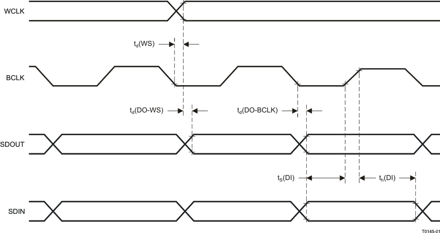 Figure 1. I2S/LJF/RJF Timing in Master Mode
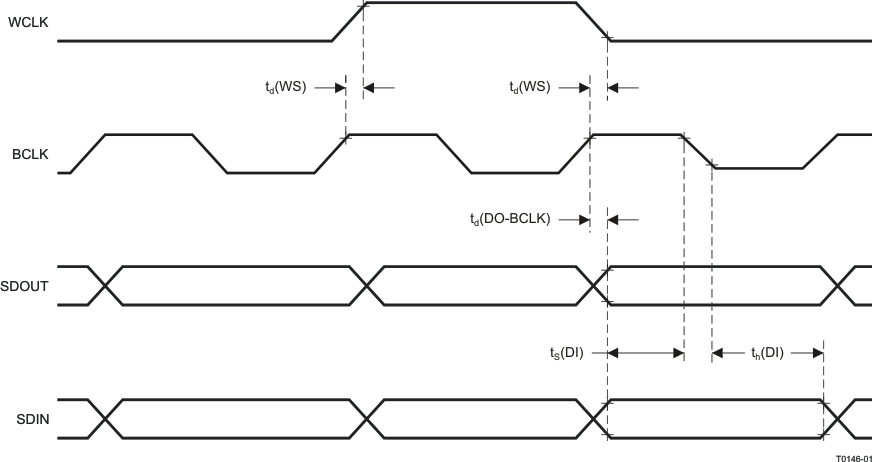 Figure 2. DSP Timing in Master Mode
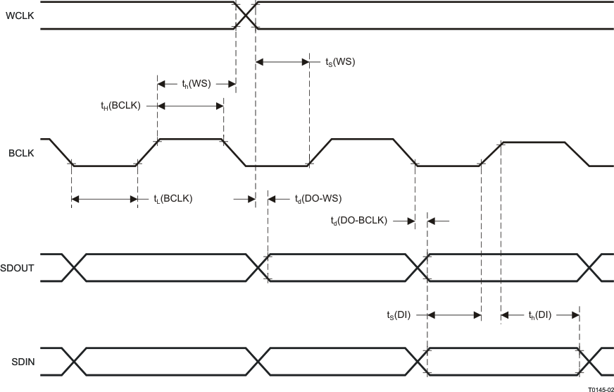 Figure 3. I2S/LJF/RJF Timing in Slave Mode
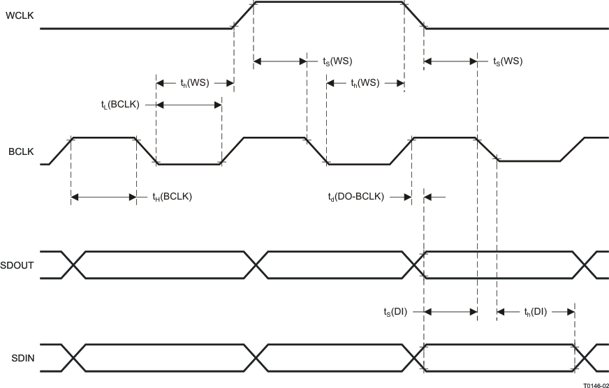 Figure 4. DSP Timing in Slave Mode
8.8 Typical Characteristics
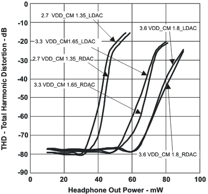 Figure 5. Total Harmonic Distortion vs Headphone Out Power
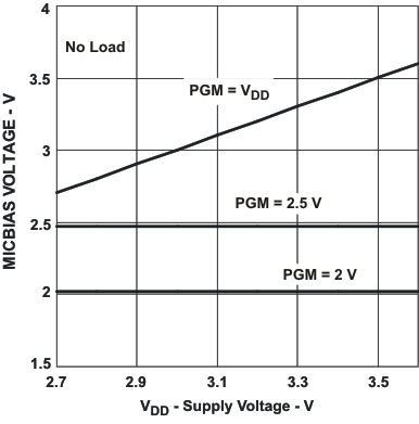 Figure 7. MICBIAS Voltage vs Supply Voltage
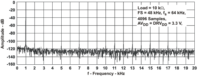 Figure 9. Left DAC FFT
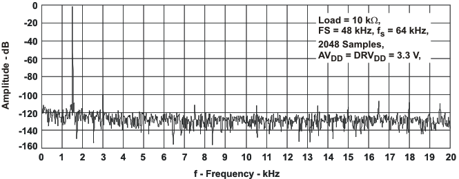 Figure 11. Left ADC FFT
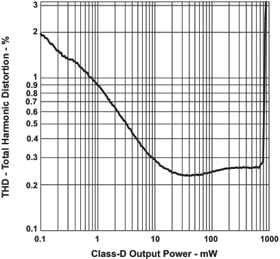 Figure 13. Total Harmonic Distortion vs Class-D Output Power
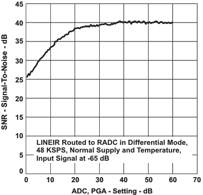 Figure 6. Signal-to-Noise Ratio vs ADC PGA Setting
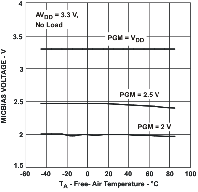 Figure 8. MICBIAS Voltage vs Free-Air Temperature
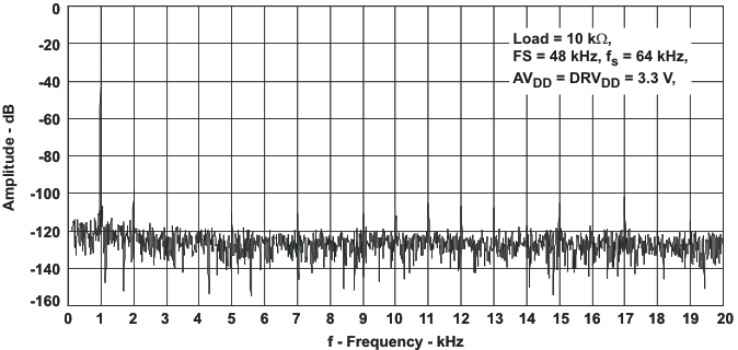 Figure 10. Right DAC FFT
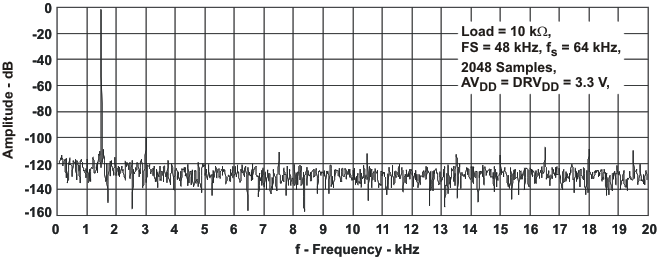 Figure 12. Right ADC FFT