-
TPA2011D1 3.2-W Mono Filter-Free Class-D Audio Power Amplifier With Auto-Recovering Short-Circuit Protection
- 1 Features
- 2 Applications
- 3 Description
- 4 Revision History
- 5 Device Comparison Table
- 6 Pin Configuration and Functions
- 7 Specifications
- 8 Parameter Measurement Information
- 9 Detailed Description
- 10Application and Implementation
- 11Power Supply Recommendations
- 12Layout
- 13Device and Documentation Support
- 14Mechanical, Packaging, and Orderable Information
- IMPORTANT NOTICE
DATA SHEET
TPA2011D1 3.2-W Mono Filter-Free Class-D Audio Power Amplifier With Auto-Recovering Short-Circuit Protection
1 Features
- Powerful Mono Class-D Amplifier
- 3.24 W (4 Ω, 5 V, 10% THDN)
- 2.57 W (4 Ω, 5 V, 1% THDN)
- 1.80 W (8 Ω, 5 V, 10% THDN)
- 1.46 W (8 Ω, 5 V, 1% THDN)
- Integrated Feedback Resistor of 300 kΩ
- Integrated Image Reject Filter for DAC Noise Reduction
- Low Output Noise of 20 μV
- Low Quiescent Current of 1.5 mA
- Auto Recovering Short-Circuit Protection
- Thermal Overload Protection
- 9-Ball, 1.21mm x 1.16 mm 0.4 mm Pitch DSBGA
2 Applications
- Wireless or Cellular Handsets and PDAs
- Portable Navigation Devices
- General Portable Audio Devices
3 Description
The TPA2011D1 is a 3.2-W high efficiency filter-free class-D audio power amplifier (class-D amp) in a 1.21 mm × 1.16 mm wafer chip scale package (DSBGA) that requires only three external components.
Features like 95% efficiency, 86-dB PSRR, 1.5 mA quiescent current and improved RF immunity make the TPA2011D1 class-D amp ideal for cellular handsets. A fast start-up time of 4 ms with no audible turn-on pop makes the TPA2011D1 ideal for PDA and smart-phone applications. The TPA2011D1 allows independent gain while summing signals from separate sources, and has a low 20 μV noise floor.
Device Information(1)
| PART NUMBER | PACKAGE | BODY SIZE (NOM) |
|---|---|---|
| TPA2011D1 | DSBGA (9) | 1.60 mm x 1.21 mm |
- For all available packages, see the orderable addendum at the end of the data sheet.
Typical Application Diagram

4 Revision History
Changes from A Revision (May 2010) to B Revision
- Added Pin Configuration and Functions section, Handling Rating table, Feature Description section, Device Functional Modes, Application and Implementation section, Power Supply Recommendations section, Layout section, Device and Documentation Support section, and Mechanical, Packaging, and Orderable Information section Go
Changes from * Revision (December 2009) to A Revision
- Changed the Package Dimensions table. D was Max = 1244μm, Min = 1184μm. E was Max = 1190μm, Min = 1130μm Go
5 Device Comparison Table
| DEVICE NUMBER | SPEAKER CHANNELS | SPEAKER AMP TYPE | OUTPUT POWER (W) | PSRR (dB) |
|---|---|---|---|---|
| TPA2011D1 | Mono | Class D | 3.2 | 86 |
| TPA2005D1 | Mono | Class D | 1.4 | 75 |
| TPA2010D1 | Mono | Class D | 2.5 | 75 |
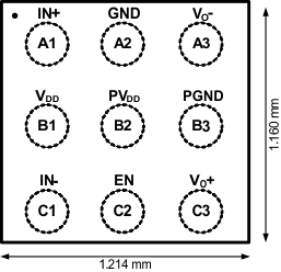
6 Pin Configuration and Functions
YFF Package
9-Pin DSBGA
Top View
Pin Functions
| PIN | I/O | DESCRIPTION | |
|---|---|---|---|
| NAME | NO. | ||
| EN | C2 | I | Shutdown terminal. When terminal is low the device is put into Shutdown mode. |
| GND | A2 | I | Analog ground terminal. Must be connected to same potential as PGND using a direct connection to a single point ground. |
| IN– | C1 | I | Negative differential audio input |
| IN+ | A1 | I | Positive differential audio input |
| PGND | B3 | I | High-current Analog ground terminal. Must be connected to same potential as GND using a direct connection to a single point ground. |
| PVDD | B2 | I | High-current Power supply terminal. Must be connected to same power supply as VDD using a direct connection. Voltage must be within values listed in Recommended Operating Conditions table. |
| VDD | B1 | I | Power supply terminal. Must be connected to same power supply as PVDD using a direct connection. Voltage must be within values listed in Recommended Operating Conditions table. |
| VO- | A3 | O | Negative BTL audio output |
| VO+ | C3 | O | Positive BTL audio output |
7 Specifications
7.1 Absolute Maximum Ratings
over operating free-air temperature range, TA = 25°C (unless otherwise noted)(1)| MIN | MAX | UNIT | |||
|---|---|---|---|---|---|
| VDD, PVDD | Supply voltage | In active mode | –0.3 | 6 | V |
| In shutdown mode | –0.3 | 6 | V | ||
| VI | Input voltage | EN, IN+, IN– | –0.3 | VDD + 0.3 | V |
| RL | Minimum load resistance | 3.2 | Ω | ||
| Output continuous total power dissipation | See Dissipation Ratings | ||||
| TA | Operating free-air temperature | –40 | 85 | °C | |
| TJ | Operating junction temperature | –40 | 150 | °C | |
| Lead temperature 1,6 mm (1/16 inch) from case for 10 seconds | 260 | °C | |||
| Tstg | Storage temperature | –65 | 85 | °C | |
(1) Stresses beyond those listed under absolute maximum ratings may cause permanent damage to the device. These are stress ratings only, and functional operation of the device at these or any other conditions beyond those indicated under recommended operating conditions is not implied. Exposure to absolute–maximum–rated conditions for extended periods may affect device reliability.
7.2 ESD Ratings
| VALUE | UNIT | |||
|---|---|---|---|---|
| V(ESD) | Electrostatic discharge | Human-body model (HBM), per ANSI/ESDA/JEDEC JS-001(1) | ±2000 | V |
| Charged-device model (CDM), per JEDEC specification JESD22-C101(2) | ±1000 | |||
(1) JEDEC document JEP155 states that 500-V HBM allows safe manufacturing with a standard ESD control process.
(2) JEDEC document JEP157 states that 250-V CDM allows safe manufacturing with a standard ESD control process.
7.3 Recommended Operating Conditions
| MIN | MAX | UNIT | |||
|---|---|---|---|---|---|
| VDD | Class-D supply voltage | 2.5 | 5.5 | V | |
| VIH | High-level input voltage | EN | 1.3 | V | |
| VIL | Low-level input voltage | EN | 0.35 | V | |
| RI | Input resistor | Gain ≤ 20 V/V (26 dB) | 15 | kΩ | |
| VIC | Common mode input voltage range | VDD = 2.5V, 5.5V, CMRR ≥ 49 dB | 0.75 | VDD-1.1 | V |
| TA | Operating free-air temperature | –40 | 85 | °C | |
7.4 Thermal Information
| THERMAL METRIC(1) | TPA2011D1 | UNIT | |
|---|---|---|---|
| YFF (DSBGA) | |||
| 9 PINS | |||
| RθJA | Junction-to-ambient thermal resistance | 107 | °C/W |
| RθJC(top) | Junction-to-case (top) thermal resistance | 0.9 | °C/W |
| RθJB | Junction-to-board thermal resistance | 18.1 | °C/W |
| ψJT | Junction-to-top characterization parameter | 3.8 | °C/W |
| ψJB | Junction-to-board characterization parameter | 18 | °C/W |
| RθJC(bot) | Junction-to-case (bottom) thermal resistance | N/A | °C/W |
(1) For more information about traditional and new thermal metrics, see the Semiconductor and IC Package Thermal Metrics application report, SPRA953.
7.5 Electrical Characteristics
TA = 25°C (unless otherwise noted)| PARAMETER | TEST CONDITIONS | MIN | TYP | MAX | UNIT | |
|---|---|---|---|---|---|---|
| |VOS| | Output offset voltage (measured differentially) | VI = 0 V, AV = 2 V/V, VDD = 2.5 V to 5.5 V | 1 | 5 | mV | |
| |IIH| | High-level input current | VDD = 5.5 V, VEN = 5.5 V | 50 | μA | ||
| |IIL| | Low-level input current | VDD = 5.5 V, VEN = 0 V | 1 | μA | ||
| I(Q) | Quiescent current | VDD = 5.5 V, no load | 1.8 | 2.5 | mA | |
| VDD = 3.6 V, no load | 1.5 | 2.3 | ||||
| VDD = 2.5 V, no load | 1.3 | 2.1 | ||||
| I(SD) | Shutdown current | VEN = 0.35 V, VDD = 2.5 V to 5.5 V | 0.1 | 2 | μA | |
| RO, SD | Output impedance in shutdown mode | VEN = 0.35 V | 2 | kΩ | ||
| f(SW) | Switching frequency | VDD = 2.5 V to 5.5 V | 250 | 300 | 350 | kHz |
| AV | Gain | VDD = 2.5 V to 5.5 V, RI in kΩ | 285/RI | 300/RI | 315/RI | V/V |
| REN | Resistance from EN to GND | 300 | kΩ | |||
7.6 Operating Characteristics
VDD = 3.6 V, TA = 25°C, AV = 2 V/V, RL = 8 Ω (unless otherwise noted)| PARAMETER | TEST CONDITIONS | MIN | TYP | MAX | UNIT | ||
|---|---|---|---|---|---|---|---|
| PO | Output power | THD + N = 10%, f = 1 kHz, RL = 4 Ω | VDD = 5 V | 3.24 | W | ||
| VDD = 3.6 V | 1.62 | ||||||
| VDD = 2.5 V | 0.70 | ||||||
| THD + N = 1%, f = 1 kHz, RL = 4 Ω | VDD = 5 V | 2.57 | W | ||||
| VDD = 3.6 V | 1.32 | ||||||
| VDD = 2.5 V | 0.57 | ||||||
| THD + N = 10%, f = 1 kHz, RL = 8 Ω | VDD = 5 V | 1.80 | W | ||||
| VDD = 3.6 V | 0.91 | ||||||
| VDD = 2.5 V | 0.42 | ||||||
| THD + N = 1%, f = 1 kHz, RL = 8 Ω | VDD = 5 V | 1.46 | W | ||||
| VDD = 3.6 V | 0.74 | ||||||
| VDD = 2.5 V | 0.33 | ||||||
| Vn | Noise output voltage | VDD = 3.6 V, Inputs AC grounded with CI = 2μF, f = 20 Hz to 20 kHz |
A-weighting | 20 | μVRMS | ||
| No weighting | 25 | ||||||
| THD+N | Total harmonic distortion plus noise | VDD = 5.0 V, PO = 1.0 W, f = 1 kHz, RL = 8 Ω | 0.11% | ||||
| VDD = 3.6 V, PO = 0.5 W, f = 1 kHz, RL = 8 Ω | 0.05% | ||||||
| VDD = 2.5 V, PO = 0.2 W, f = 1 kHz, RL = 8 Ω | 0.05% | ||||||
| VDD = 5.0 V, PO = 2.0 W, f = 1 kHz, RL = 4 Ω | 0.23% | ||||||
| VDD = 3.6 V, PO = 1.0 W, f = 1 kHz, RL = 4 Ω | 0.07% | ||||||
| VDD = 2.5 V, PO = 0.4 W, f = 1 kHz, RL = 4 Ω | 0.06% | ||||||
| PSRR | AC power supply rejection ratio | VDD = 3.6 V, Inputs AC grounded with CI = 2 μF, 200 mVpp ripple, f = 217 Hz |
86 | dB | |||
| CMRR | Common mode rejection ratio | VDD = 3.6 V, VIC = 1 VPP, f = 217 Hz | 79 | dB | |||
| TSU | Startup time from shutdown | VDD = 3.6 V | 4 | ms | |||
| IOC | Overcurrent protection threshold | VDD = 3.6 V, VO+ shorted to VDD | 2 | A | |||
| VDD = 3.6 V, VO– shorted to VDD | 2 | ||||||
| VDD = 3.6 V, VO+ shorted to GND | 2 | ||||||
| VDD = 3.6 V, VO– shorted to GND | 2 | ||||||
| VDD = 3.6 V, VO+ shorted to VO– | 2 | ||||||
| TSD | Time for which output is disabled after a short-circuit event, after which auto-recovery trials are continuously made | VDD = 2.5 V to 5.5 V | 100 | ms | |||
7.7 Dissipation Ratings
| PACKAGE | DERATING FACTOR(1) | TA < 25°C | TA = 70°C | TA = 85°C |
|---|---|---|---|---|
| YFF (DSBGA) | 4.2 mW/°C | 525 mW | 336 mW | 273 mW |
(1) Derating factor measure with high K board.
7.8 Typical Characteristics
VDD = 3.6 V, CI = 0.1 μF, CS1 = 0.1 μF, CS2 = 10 μF, TA = 25°C, RL = 8 Ω (unless otherwise noted)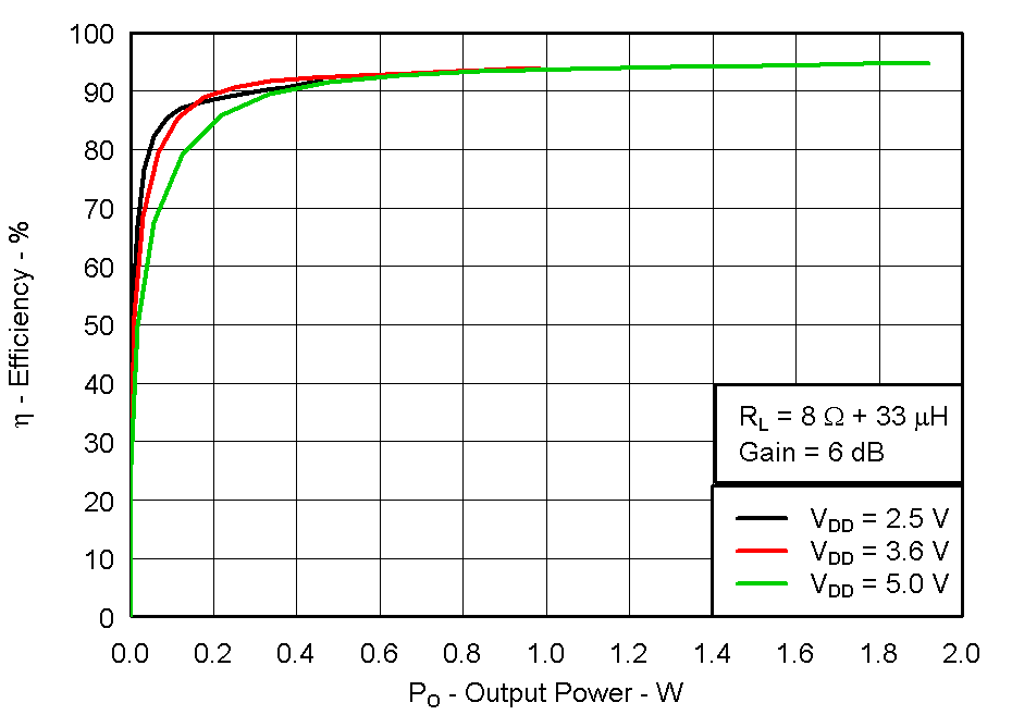 Figure 1. Efficiency vs Output Power
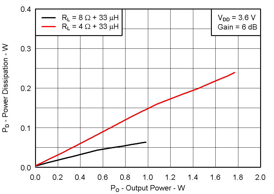 Figure 3. Power Dissipation vs Output Power
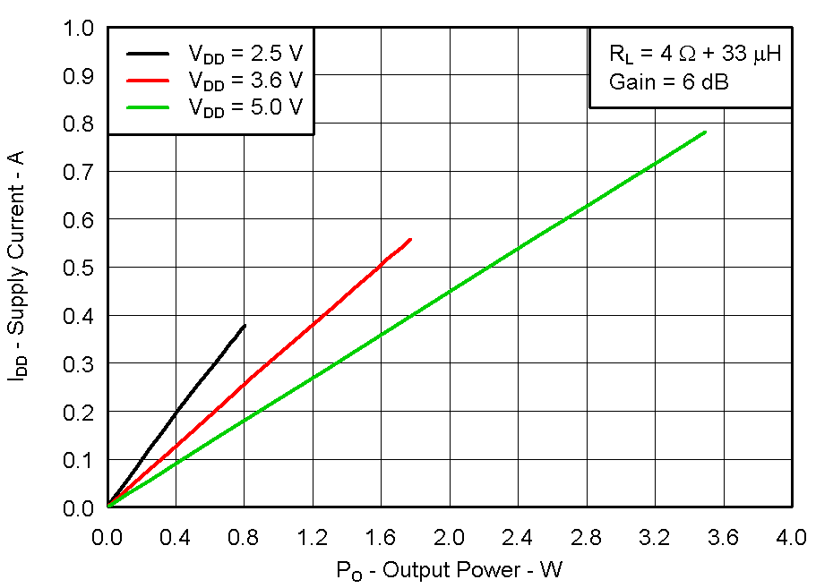 Figure 5. Supply Current vs Output Power
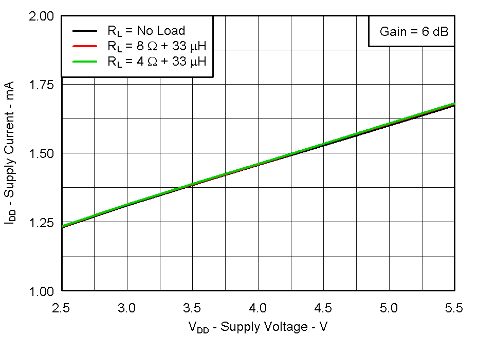 Figure 7. Supply Current vs Supply Voltage
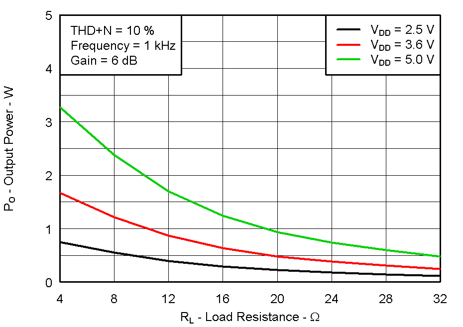 Figure 9. Output Power vs Load Resistance
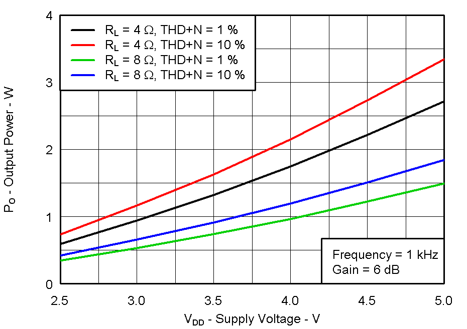 Figure 11. Output Power vs Supply Resistance
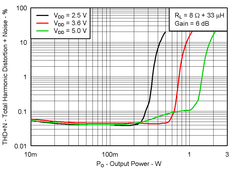 Figure 13. THD + Noise vs Output Power
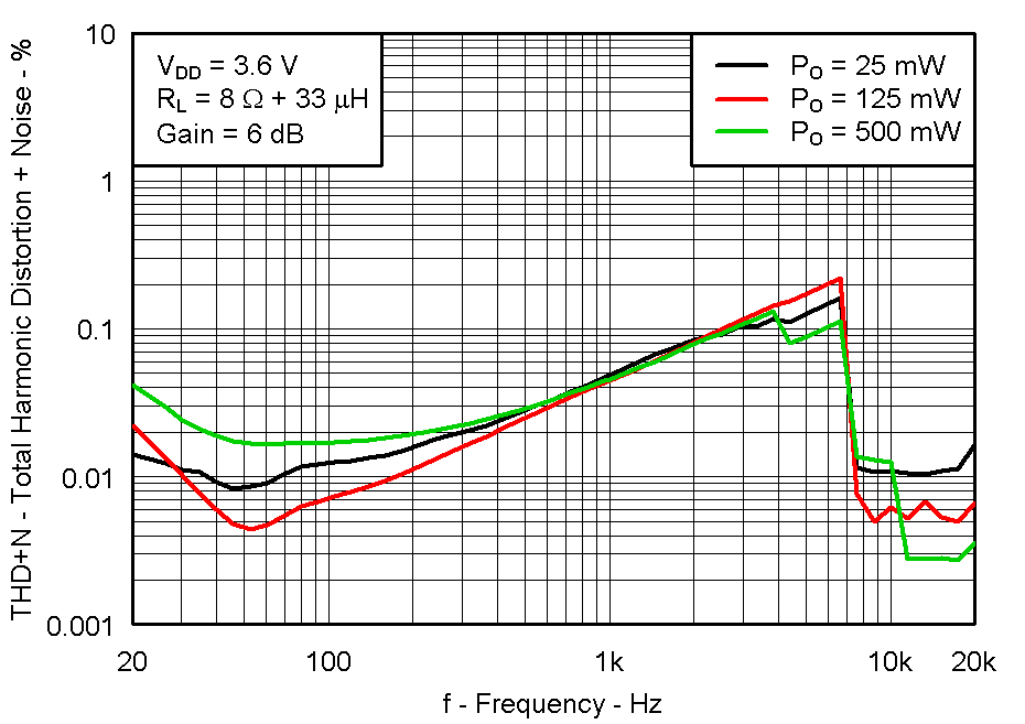 Figure 15. THD + Noise vs Frequency
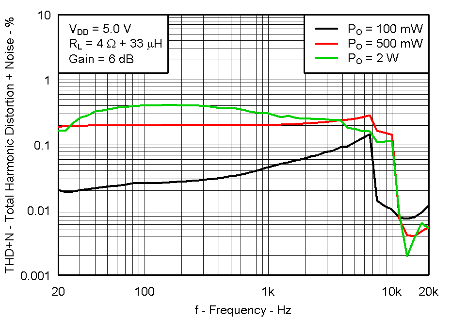 Figure 17. THD + Noise vs Frequency
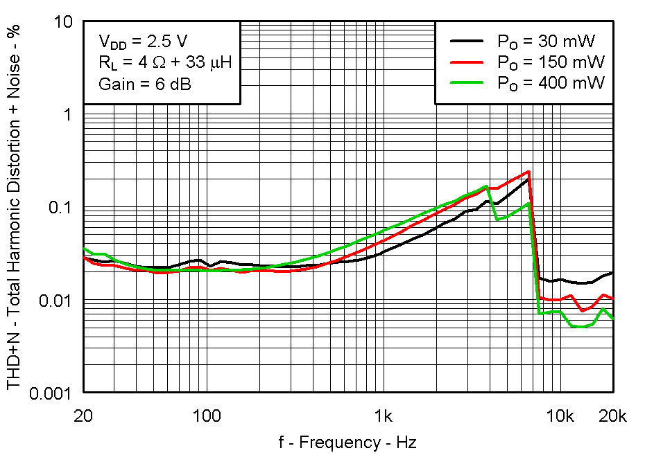 Figure 19. THD + Noise vs Frequency
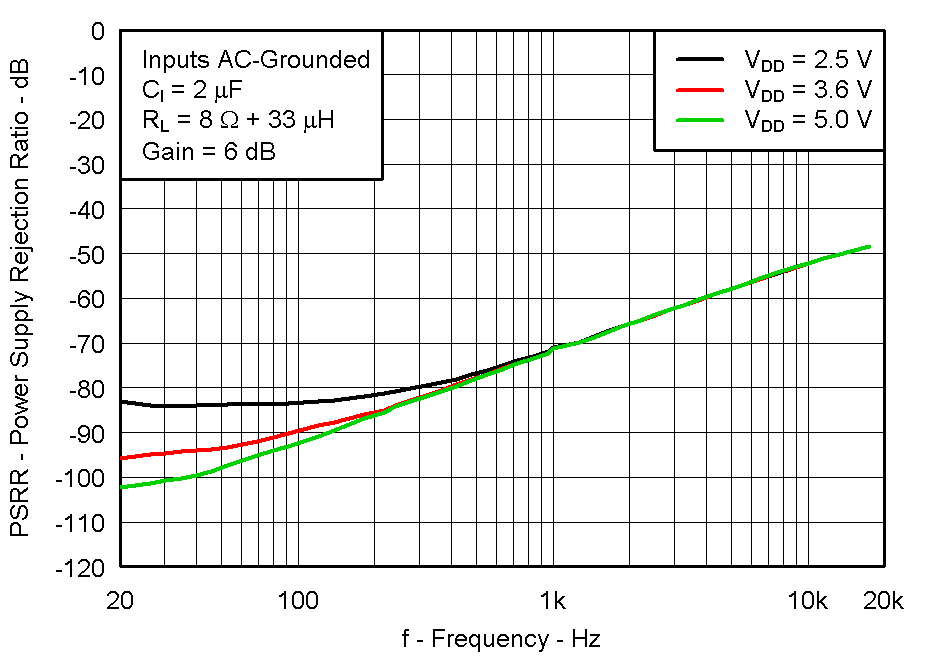 Figure 21. Power Supply Rejection Ratio vs Frequency
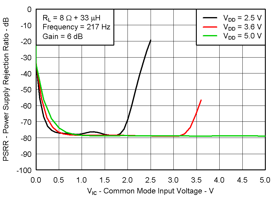 Figure 23. Power Supply Rejection Ratio vs Common Mode Input Voltage
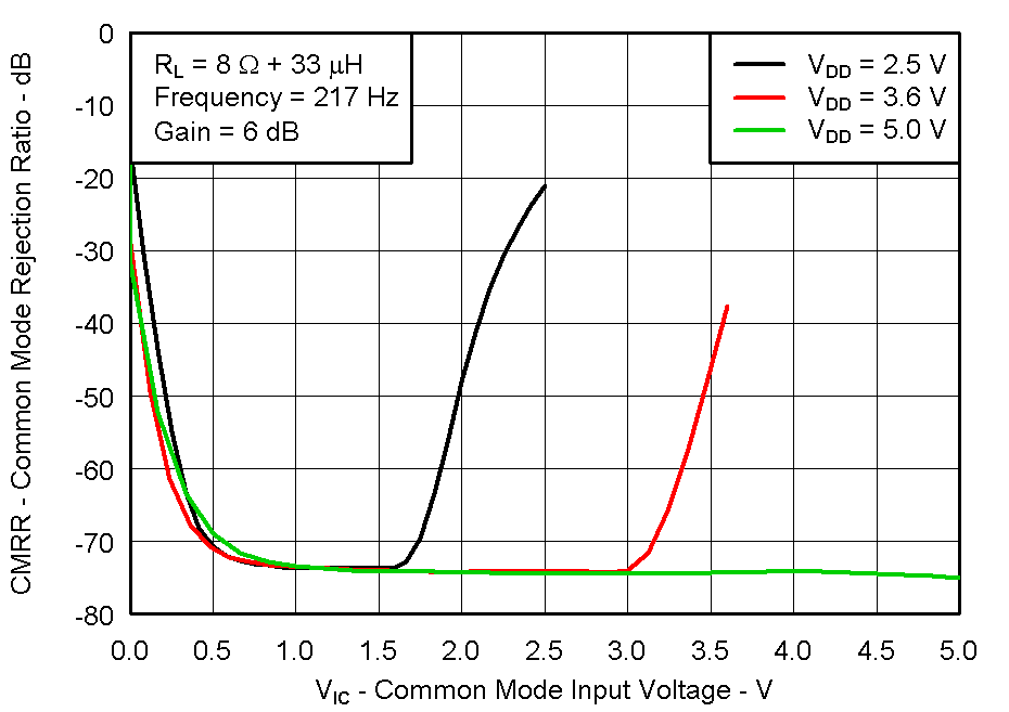 Figure 25. Common Mode Rejection Ratio vs Common Mode Input Voltage
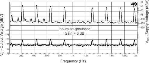 Figure 27. GSM Power Supply Rejection vs Frequency
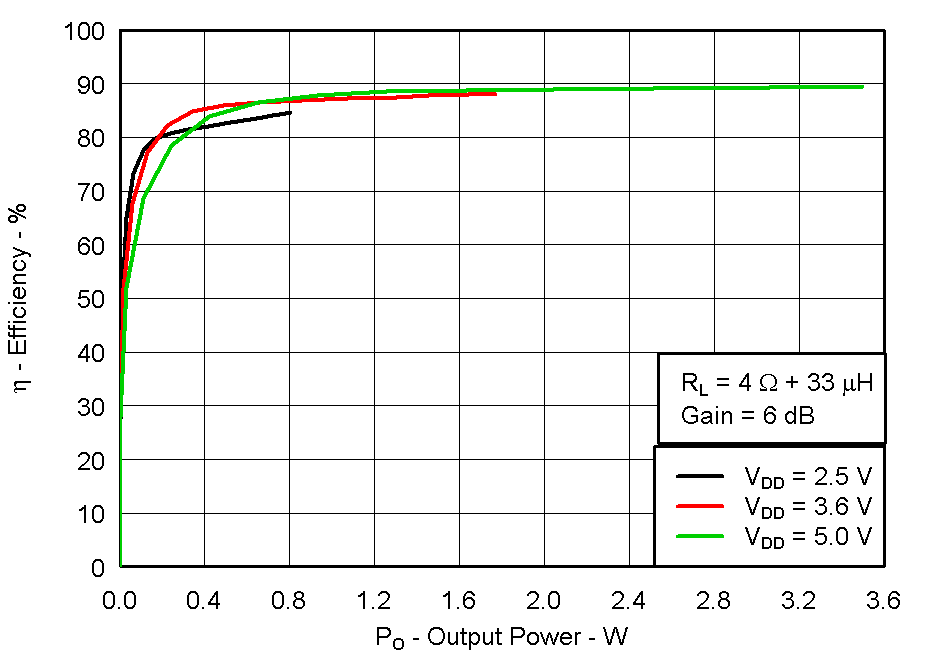 Figure 2. Efficiency vs Output Power
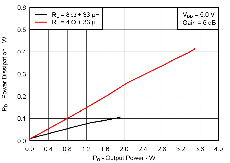 Figure 4. Power Dissipation vs Output Power
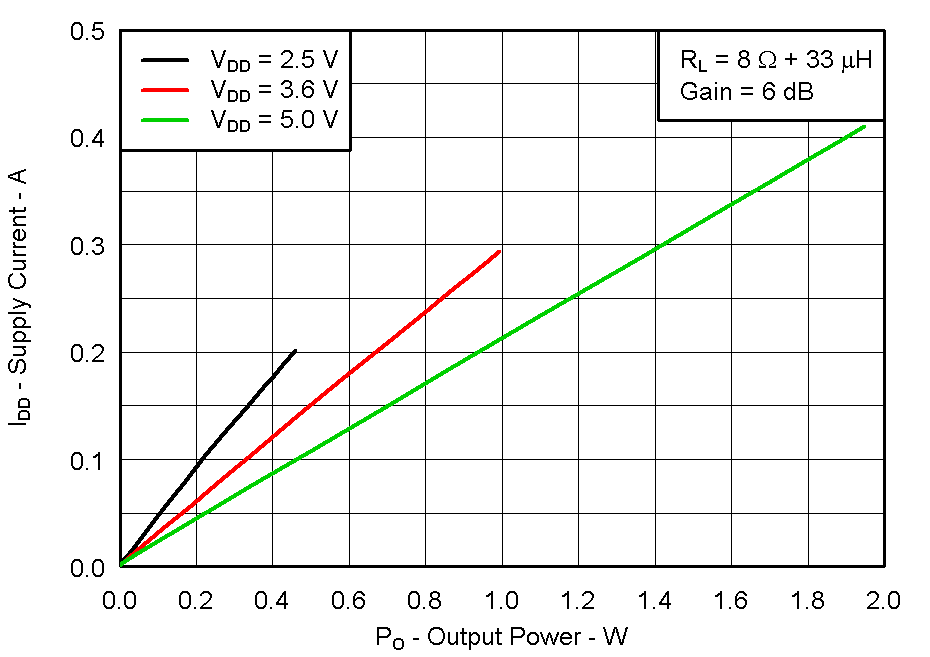 Figure 6. Supply Current vs Output Power
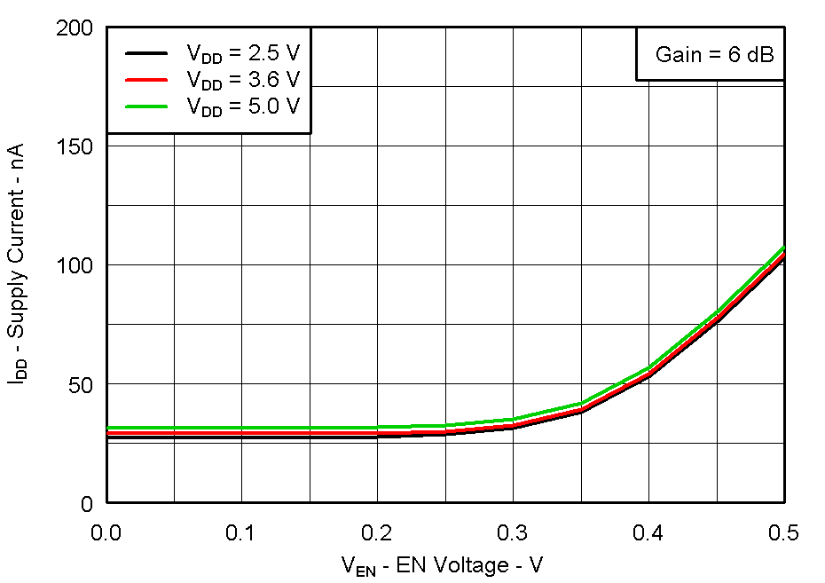 Figure 8. Supply Current vs EN Voltage
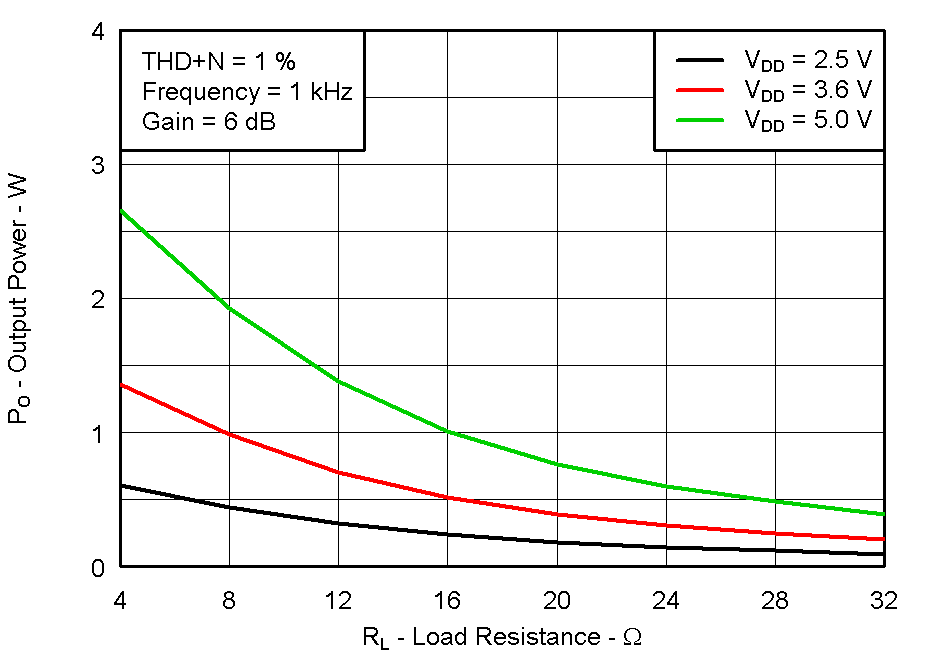 Figure 10. Output Power vs Load Resistance
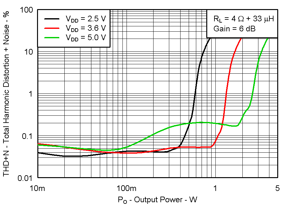 Figure 12. THD + Noise vs Output Power
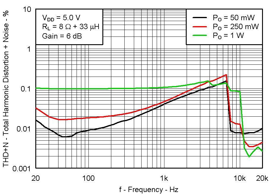 Figure 14. THD + Noise vs Frequency
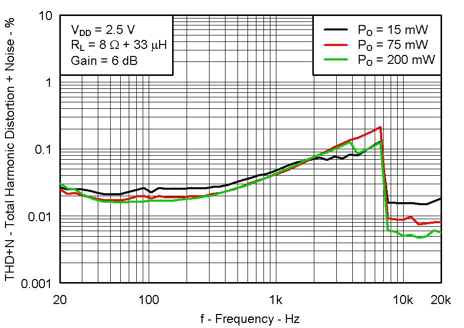 Figure 16. THD + Noise vs Frequency
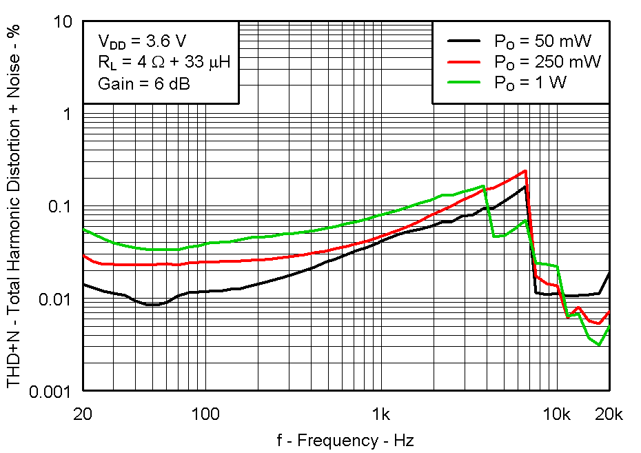 Figure 18. THD + Noise vs Frequency
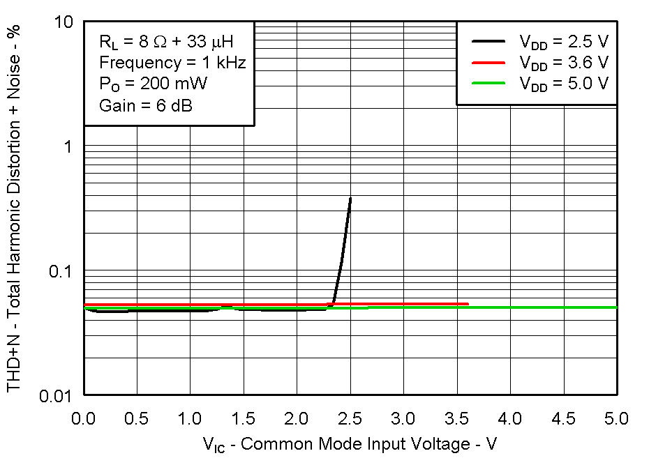 Figure 20. THD + Noise vs Common Mode Input Voltage
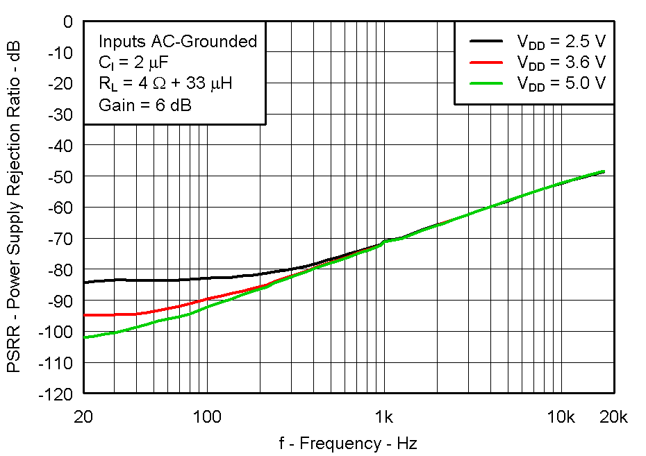 Figure 22. Power Supply Rejection Ratio vs Frequency
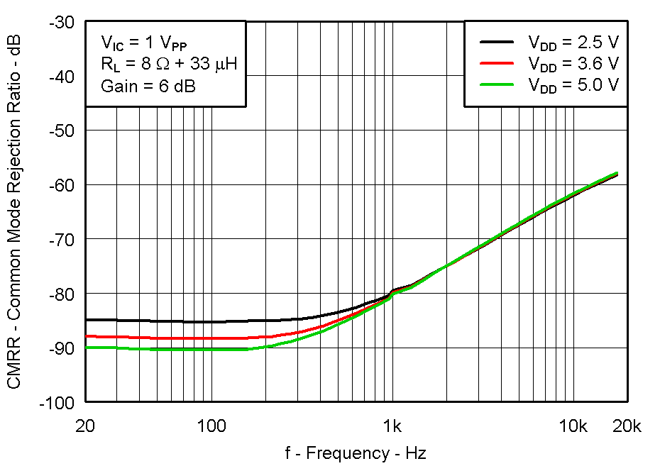 Figure 24. Common Mode Rejection Ratio vs Frequency
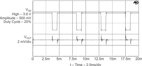 Figure 26. GSM Power Supply Rejection vs Time