SLOS930C November   2015  – October 2024 THS4541-Q1

PRODUCTION DATA  

  1.   1
  2. Features
  3. Applications
  4. Description
  5. Device Comparison Table
  6. Pin Configuration and Functions
  7. Specifications
    1. 6.1 Absolute Maximum Ratings
    2. 6.2 ESD Ratings
    3. 6.3 Recommended Operating Conditions
    4. 6.4 Thermal Information
    5. 6.5 Electrical Characteristics: (Vs+) – Vs– = 5 V
    6. 6.6 Electrical Characteristics: (Vs+) – Vs– = 3 V
    7. 6.7 Typical Characteristics: 5-V Single Supply
    8. 6.8 Typical Characteristics: 3-V Single Supply
    9. 6.9 Typical Characteristics: 3-V to 5-V Supply Range
  8. Parameter Measurement Information
    1. 7.1 Example Characterization Circuits
    2. 7.2 Frequency-Response Shape Factors
    3. 7.3 I/O Headroom Considerations
    4. 7.4 Output DC Error and Drift Calculations and the Effect of Resistor Imbalances
    5. 7.5 Noise Analysis
    6. 7.6 Factors Influencing Harmonic Distortion
    7. 7.7 Driving Capacitive Loads
    8. 7.8 Thermal Analysis
  9. Detailed Description
    1. 8.1 Overview
      1. 8.1.1 Terminology and Application Assumptions
    2. 8.2 Functional Block Diagram
    3. 8.3 Feature Description
      1. 8.3.1 Differential I/O
      2. 8.3.2 Power-Down Control Pin ( PD)
        1. 8.3.2.1 Operating the Power Shutdown Feature
      3. 8.3.3 Input Overdrive Operation
    4. 8.4 Device Functional Modes
      1. 8.4.1 Operation from Single-Ended Sources to Differential Outputs
        1. 8.4.1.1 AC-Coupled Signal Path Considerations for Single-Ended Input to Differential Output Conversion
        2. 8.4.1.2 DC-Coupled Input Signal Path Considerations for Single-Ended to Differential Conversion
        3. 8.4.1.3 Resistor Design Equations for the Single-Ended to Differential Configuration of the FDA
        4. 8.4.1.4 Input Impedance for the Single-Ended to Differential FDA Configuration
      2. 8.4.2 Differential-Input to Differential-Output Operation
        1. 8.4.2.1 AC-Coupled, Differential-Input to Differential-Output Design Issues
        2. 8.4.2.2 DC-Coupled, Differential-Input to Differential-Output Design Issues
  10. Application and Implementation
    1. 9.1 Application Information
    2. 9.2 Typical Applications
      1. 9.2.1 Designing Attenuators
        1. 9.2.1.1 Design Requirements
        2. 9.2.1.2 Detailed Design Procedure
        3. 9.2.1.3 Application Curve
      2. 9.2.2 Interfacing to High-Performance ADCs
        1. 9.2.2.1 Design Requirements
        2. 9.2.2.2 Detailed Design Procedure
        3. 9.2.2.3 Application Curve
    3. 9.3 Power Supply Recommendations
    4. 9.4 Layout
      1. 9.4.1 Layout Guidelines
      2. 9.4.2 Layout Example
  11. 10Device and Documentation Support
    1. 10.1 Device Support
      1. 10.1.1 Development Support
        1. 10.1.1.1 TINA Simulation Model Features
    2. 10.2 Documentation Support
      1. 10.2.1 Related Documentation
    3. 10.3 Receiving Notification of Documentation Updates
    4. 10.4 Support Resources
    5. 10.5 Trademarks
    6. 10.6 Electrostatic Discharge Caution
    7. 10.7 Glossary
  12. 11Revision History
  13. 12Mechanical, Packaging, and Orderable Information

Typical Characteristics: 3-V to 5-V Supply Range

at Vs+ = 3 V and 5 V, Vs– = GND, Vocm is open, 50-Ω single-ended input to differential output, gain = 2 V/V, Rload = 500 Ω, and TA ≈ 25°C (unless otherwise noted)
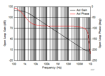
THS4541-Q1 Main
                        Amplifier Differential Open-Loop Gain and Phase vs Frequency


Figure 6-37 Main Amplifier Differential Open-Loop Gain and Phase vs Frequency
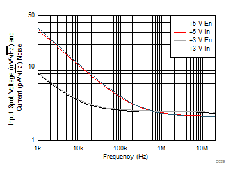
THS4541-Q1 Input
                        Spot Noise Over Frequency
 
 
Figure 6-39 Input Spot Noise Over Frequency
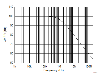
THS4541-Q1 CMRR
                        Over Frequency
Common-mode in to differential out, gain of 2 simulation
 
Figure 6-41 CMRR Over Frequency
THS4541-Q1 Common-Mode, Small- and Large-Signal Response (Vocm pin driven)
 
Figure 6-43 Common-Mode, Small- and Large-Signal Response (Vocm pin driven)
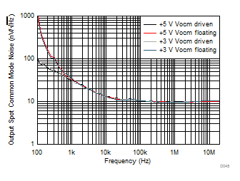
THS4541-Q1 Output Common-Mode Noise
Vocm input either driven to midsupply by low impedance source, or allowed to float and default to midsupply
Figure 6-45 Output Common-Mode Noise
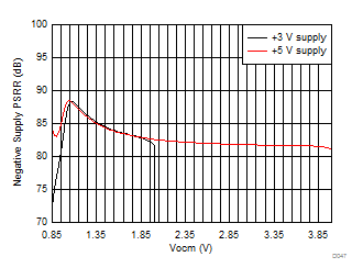
THS4541-Q1 –PSRR
                        vs Vocm Approaching Vs–
Single-ended to differential gain of 2 (see Figure 7-1), PSRR for negative supply to differential output (1-kHz simulation)
Figure 6-47 –PSRR vs Vocm Approaching Vs–
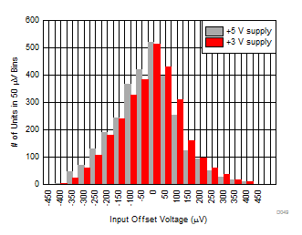
THS4541-Q1 Input
                        Offset Voltage
3 lots, total of 2962 units trimmed at 5-V supply
Figure 6-49 Input Offset Voltage
THS4541-Q1 Input
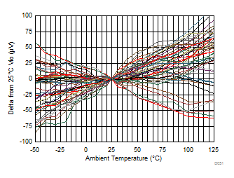
                        Offset Voltage Over Temperature
5-V and 3-V delta from 25°C VIO, 25 units
Figure 6-51 Input Offset Voltage Over Temperature
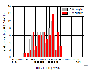
THS4541-Q1 Input
                        Offset Voltage Drift
–40°C to +125°C endpoint drift, 3 lots, total of 68 units
Figure 6-53 Input Offset Voltage Drift
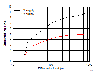
THS4541-Q1 Maximum Vopp vs Rload
Maximum differential output swing, Vocm at midsupply
Figure 6-55 Maximum Vopp vs Rload
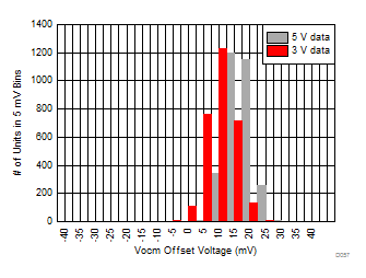
THS4541-Q1 Common-Mode Output Offset from Vs+ / 2 Default Value
 
Vocm input floating, 3 lots, total of 2962 units
Figure 6-57 Common-Mode Output Offset from Vs+ / 2 Default Value
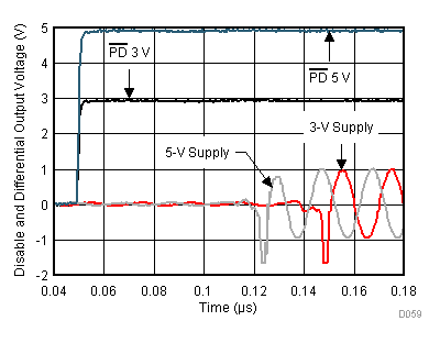
THS4541-Q1 PD Turn On Waveform
10 MHz, 1-Vpp input single to differential gain of 2,
see Figure 7-3
Figure 6-59 PD Turn On Waveform
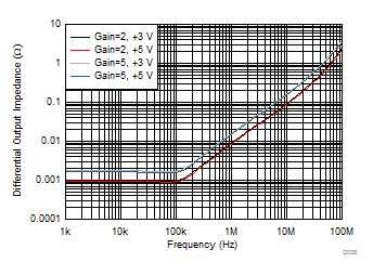
THS4541-Q1 Closed-Loop Output Impedance
Single-ended input to differential output, simulated differential output impedance, (closed-loop) gain of 2 and 5,
see Figure 7-1
Figure 6-38 Closed-Loop Output Impedance
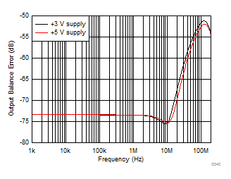
THS4541-Q1 Output Balance Error Over Frequency
Single-ended input to differential output, gain of 2 (see Figure 7-1), simulated with 1% resistor, worst-case mismatch
Figure 6-40 Output Balance Error Over Frequency
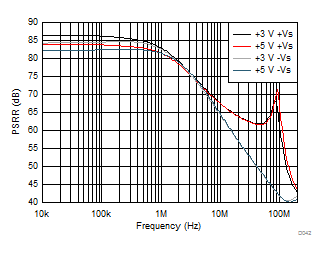
THS4541-Q1 PSRR
                        Over Frequency
Single-ended to differential, gain of 2 (see Figure 7-1)
PSRR simulated to differential output
Figure 6-42 PSRR Over Frequency
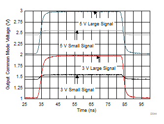
THS4541-Q1 Common-Mode, Small- and Large-Step Response (Vocm pin driven)
 
Figure 6-44 Common-Mode, Small- and Large-Step Response (Vocm pin driven)
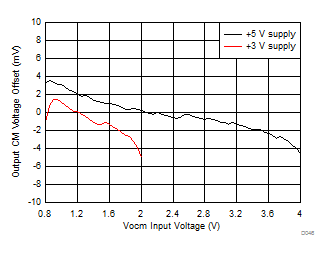
THS4541-Q1 Vocm
                        Offset vs Vocm Setting
Average Vocm output offset of 37 units,
standard deviation < 2.5 mV, see Figure 7-3
Figure 6-46 Vocm Offset vs Vocm Setting
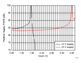
THS4541-Q1 +PSRR
                        vs Vocm Approaching Vs+
Single-ended to differential gain of 2 (see Figure 7-1), PSRR for positive supply to differential output (1-kHz simulation)
Figure 6-48 +PSRR vs Vocm Approaching Vs+
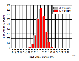
THS4541-Q1 Input
                        Offset Current
3 lots, total of 2962 units
Figure 6-50 Input Offset Current
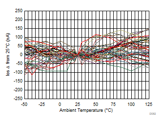
THS4541-Q1 Input
                        Offset Current Over Temperature
5-V and 3-V over temperature IOS, 25 units
Figure 6-52 Input Offset Current Over Temperature
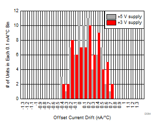
THS4541-Q1 Input
                        Offset Current Drift
–40°C to +125°C endpoint drift, 3 lots, total of 68 units
Figure 6-54 Input Offset Current Drift
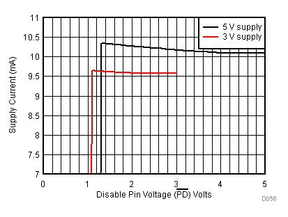
THS4541-Q1 Supply Current vs PD Voltage
 
Figure 6-56 Supply Current vs PD Voltage
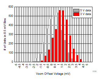
THS4541-Q1 Common-Mode Output Offset from Driven Vocm
Input driven midsupply, 3 lots, total of 2962 units
Figure 6-58 Common-Mode Output Offset from Driven Vocm
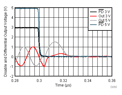
THS4541-Q1 PD Turn Off Waveform
10 MHz, 1-VPP input single to differential gain of 2,
see Figure 7-3
Figure 6-60 PD Turn Off Waveform