SLOSEC9 September   2024 TSD5402-Q1

PRODUCTION DATA  

  1.   1
  2. Features
  3. Applications
  4. Description
  5. Pin Configuration and Functions
  6. Specifications
    1. 5.1 Absolute Maximum Ratings
    2. 5.2 ESD Ratings
    3. 5.3 Recommended Operating Conditions
    4. 5.4 Thermal Information
    5. 5.5 Electrical Characteristics
    6. 5.6 Timing Requirements for I2C Interface Signals
    7. 5.7 Typical Characteristics
  7. Detailed Description
    1. 6.1 Overview
    2. 6.2 Functional Block Diagram
    3. 6.3 Feature Description
      1. 6.3.1 Analog Input and Preamplifier
      2. 6.3.2 Pulse-Width Modulator (PWM)
      3. 6.3.3 Gate Drive
      4. 6.3.4 Power FETs
      5. 6.3.5 Load Diagnostics
        1. 6.3.5.1 Load Diagnostics Sequence
        2. 6.3.5.2 Faults During Load Diagnostics
      6. 6.3.6 Protection and Monitoring
      7. 6.3.7 I2C Serial Communication Bus
        1. 6.3.7.1 I2C Bus Protocol
        2. 6.3.7.2 Random Write
        3. 6.3.7.3 Random Read
        4. 6.3.7.4 Sequential Read
    4. 6.4 Device Functional Modes
      1. 6.4.1 Hardware Control Pins
      2. 6.4.2 EMI Considerations
      3. 6.4.3 Operating Modes and Faults
  8. Register Maps
    1. 7.1 I2C Address Register Definitions
  9. Application and Implementation
    1. 8.1 Application Information
    2. 8.2 Typical Application
      1. 8.2.1 Design Requirements
        1. 8.2.1.1 Amplifier Output Filtering
        2. 8.2.1.2 Amplifier Output Snubbers
        3. 8.2.1.3 Bootstrap Capacitors
        4. 8.2.1.4 Analog Signal Input Filter
      2. 8.2.2 Detailed Design Procedure
        1. 8.2.2.1 Unused Pin Connections
          1. 8.2.2.1.1 HI-Z Pin
          2. 8.2.2.1.2 STANDBY Pin
          3. 8.2.2.1.3 I2C Pins (SDA and SCL)
          4. 8.2.2.1.4 Terminating Unused Outputs
          5. 8.2.2.1.5 Using a Single-Ended Signal Input
      3. 8.2.3 Application Curves
    3. 8.3 Power Supply Recommendations
    4. 8.4 Layout
      1. 8.4.1 Layout Guidelines
      2. 8.4.2 Layout Examples
        1. 8.4.2.1 Top Layer
        2. 8.4.2.2 Second Layer – Signal Layer
        3. 8.4.2.3 Third Layer – Power Layer
        4. 8.4.2.4 Bottom Layer – Ground Layer
  10. Device and Documentation Support
    1. 9.1 Device Support
      1. 9.1.1 Third-Party Products Disclaimer
    2. 9.2 Documentation Support
      1. 9.2.1 Related Documentation
    3. 9.3 Receiving Notification of Documentation Updates
    4. 9.4 Support Resources
    5. 9.5 Trademarks
    6. 9.6 Electrostatic Discharge Caution
    7. 9.7 Glossary
  11. 10Revision History
  12. 11Mechanical, Packaging, and Orderable Information
    1. 11.1 Package Option Addendum
      1. 11.1.1 Packaging Information
      2. 11.1.2 Tape and Reel Information

Typical Characteristics

TC = 25°C, PVDD = 14.4 V, RL = 4 Ω, P(O) = 1 W per channel, AES17 filter, 1-kHz input, default I2C settings (unless otherwise noted)
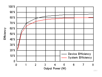
TSD5402-Q1 Efficiency vs Output Power
f(SW) = 400 kHzTA = 25°CV(PVDD) = 14.4 V
Figure 5-1 Efficiency vs Output Power
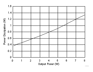
TSD5402-Q1 Power Dissipation vs Output Power
Figure 5-3 Power Dissipation vs Output Power
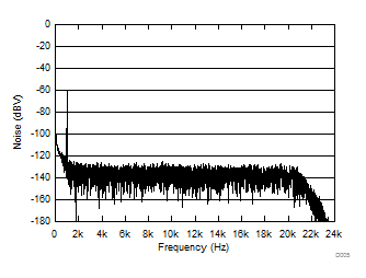
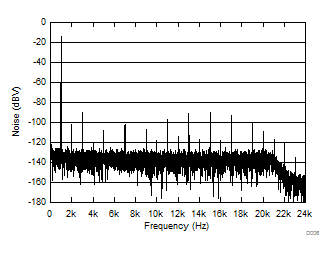
TSD5402-Q1 Noise FFT With –60-dB Output
Figure 5-5 Noise FFT With –60-dB Output
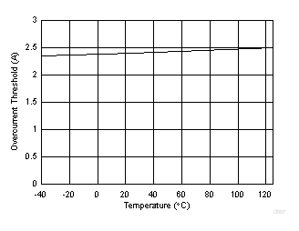
TSD5402-Q1 Overcurrent Threshold vs Temperature
Figure 5-7 Overcurrent Threshold vs Temperature
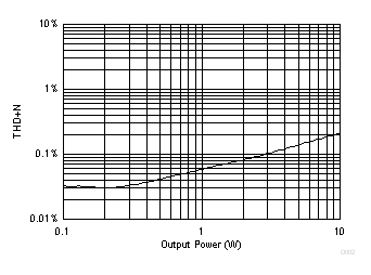
TSD5402-Q1 THD+N vs Output Power
Figure 5-2 THD+N vs Output Power
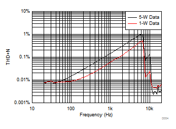
TSD5402-Q1 THD+N vs Frequency
Figure 5-4 THD+N vs Frequency
TSD5402-Q1 Noise FFT With 1-W Output
Figure 5-6 Noise FFT With 1-W Output