Understanding Power Module Operating Limits
Trademarks
All trademarks are the property of their respective owners.
1 Introduction
Open any power module data sheet and its front page will advertise the module’s load current capability and input and output voltage range. A module with selectable or adjustable switching frequency will advertise its frequency options on the data sheet front page as well. In reality, not all input voltage, output voltage, load current, and switching frequency combinations can be achieved due to timing, current, and thermal limitations. One must look further into the datasheet to better comprehend the module’s valid operating conditions.
Power module data sheets include tables and graphs that summarize the maximum load current capability for different input and output voltage ranges, and different switching frequencies, if selectable/adjustable. An example of such a table is shown in Table 1-1 for the TPSM5D1806, which is a dual 6-A output buck power module with four selectable switching frequencies: 500kHz, 1MHz, 1.5MHz, and 2MHz. With this table, one can quickly determine the possible switching frequency choices for a desired input to output voltage conversion and max load current requirement, without needing to perform any calculations and analysis by hand or experimentally. Furthermore, module data sheets provide Safe Operating Area (SOA) curves, which show the maximum allowed ambient temperature versus load current as measured on the evaluation board (EVM), as an aid to quantifying the thermal capabilities of the device.
While these data sheet tables and graphs are useful for quick analysis and assessment of the device’s capabilities, they may leave an engineer wanting a deeper understanding of how the operating boundaries of the module have been determined. This understanding can aid an engineer in better selecting, comparing, and configuring power modules for their designs.
| Output Current per Channel | Switching Frequency (kHz) | VIN = 5 V | VIN = 12 V | ||
|---|---|---|---|---|---|
| VOUT RANGE | VOUT RANGE | ||||
| MIN | MAX | MIN | MAX | ||
| 6 A | 500 | - | - | 0.5 | 0.8 |
| 1000 | 0.5 | 0.8 | 0.7 | 1.6 | |
| 1500 | 0.5 | 1.3 | 1.0 | 2.4 | |
| 2000 | 0.6 | 1.8 | 1.4 | 3.2 | |
| 5 A | 500 | 0.5 | 0.8 | 0.5 | 0.9 |
| 1000 | 0.5 | 1.8 | 0.7 | 2.0 | |
| 1500 | 0.5 | 3.3 | 1.0 | 3.6 | |
| 2000 | 0.6 | 2.8 | 1.4 | 5.5 | |
| ≤ 4 A | 500 | 0.5 | 0.9 | 0.5 | 0.9 |
| 1000 | 0.5 | 3.9 | 0.7 | 2.0 | |
| 1500 | 0.5 | 3.5 | 1.0 | 3.6 | |
| 2000 | 0.6 | 2.8 | 1.4 | 5.5 | |
2 Basic Buck Regulator Operation
The fundamental operation of buck regulators is discussed in detail in other application reports (3). While not covered in detail here, an understanding of the basic buck operational waveforms is useful for the discussions in this report. Figure 2-1 shows the basic synchronous buck power stage and the simplified waveforms of the inductor current (iL) and switching node (vSW) in steady state continuous-conduction mode (CCM) conditions. For simplicity, dead times and resistive components such as MOSFET on-resistances and the inductor DC resistance have not been considered in the analyses and equations in this report.
During the on time, tON, the high-side (HS) MOSFET is on and the low-side (LS) MOSFET is off. In this state, a positive voltage VIN-VOUT exists across the inductor, which causes the inductor current to ramp up. During the off-time, tOFF, the HS MOSFET is off and LS MOSFET is on. With the switching node at ground, the voltage across the inductor is -VOUT, which causes the inductor current to ramp back down. The switching period, tSW, is the sum of tON and tOFF and is the inverse of the switching frequency, FSW. The duty cycle, D, can be defined as D = tON / tSW. In a real buck regulator, the on and off times are dynamically set by the buck’s control loop circuitry, which then generates signals to the gate drivers that turn the power MOSFETs on and off.

Figure 2-1 Basic synchronous buck regulator and waveforms
3 Impact of Minimum On-Time and Minimum Off-Time
Buck regulators have a minimum on-time and minimum off-time (4) that are the result of gate drive circuitry limitations, control and drive circuit delays, and intentional blanking times. For example, for peak current mode devices with HS MOSFET current sensing, there is a surge in current flowing in the HS FET during its turn-on transition to provide the charge for the LS FET body diode reverse recovery. An initial blanking time in the current sense circuit at the FET turn-on ensures a clean representation of the current is used by the control loop and protection circuitry.
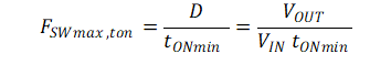
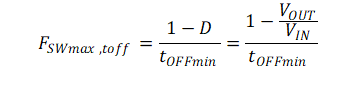
A regulator's minimum on-time and minimum off-time set maximum limits to the allowed switching frequency as defined by Equation 1 and Equation 2 (ignoring resistive voltage drops):
The TPSM5D1806 has a typical minimum on-time, tONmin, of 30 ns and minimum off-time, tOFFmin, of 150 ns. Adding some design margin to typical values is recommended, so values of tONmin of 50 ns and tOFFmin of 200 ns are more conservative numbers used for analysis. Taking an example condition of VIN = 12 V and VOUT = 1 V, the maximum theoretical frequency allowed due to minimum on-time is 1.67 MHz, and maximum theoretical frequency due to minimum off-time is 4.58 MHz. While the minimum off-time is not imposing a limit in this example, the minimum on-time does prohibit the use of the 2-MHz switching frequency option.
When selecting a frequency option for a device with fixed discrete frequency options such as the TPSM5D1806, it is recommended to consider the frequency tolerance as well. The frequency tolerance of the internal oscillator is ±10%, which implies that a device set to 1.5 MHz may have an actual frequency of up to 1.65 MHz, which is close to the 1.67-MHz limit calculated due to min on-time in the previous example. Frequency synchronization to an external clock with tighter accuracy can reduce the required design margins to avoid minimum on- and off-time violations. If the input supply has a wide tolerance or is not well regulated, the maximum and minimum input voltages should be considered when analyzing the maximum allowed frequencies due to minimum on-time and off-time, respectively.
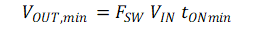
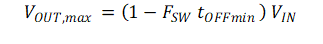
The maximum frequency equations can also be rearranged as Equation 3 and Equation 4 to define the minimum output voltage allowed due to minimum on-time and the maximum output voltage due to minimum off-time at a given frequency and input voltage. The output voltage range due to timing limitations can then be plotted as shown in Figure 3-1 for the TPSM5D1806 at an input voltage of 12 V. The min and max are clamped to the specified output voltage range of the device of 0.5 V to 5.5 V. This figure then makes it easy to read the output voltage range at a given frequency; for example, at 1-MHz switching frequency, the theoretical output voltage range considering only minimum on- and off-times and the basic voltage range limits is 0.7 V to 5.5 V.
")
Figure 3-1 TPSM5D1806 Output Voltage Range Due to Minimum On- and Off-Time Only (VIN = 12 V)
4 Impact of Current Limits
Every practical voltage regulator requires current limits to protect its components such as power MOSFETs, inductor, and wiring, which all have inherent maximum current ratings (5).
To the first order, inductor ripple, IPP, and peak inductor or HS FET current, IPEAK, are given by Equation 5 and Equation 6. A HS overcurrent limit typically acts to shut off the buck HS FET when the sensed FET or inductor current hits the current limit value.
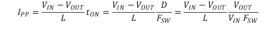
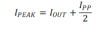
Given a HS overcurrent limit, IHS,OC, the maximum allowed load current is given by Equation 7. In a buck power module where the inductor is fixed, the free variables that influence ripple current are input voltage, output voltage, and switching frequency. For duty cycles below 50%, increasing VOUT or increasing VIN will increase IPP and reduce the maximum allowed load current before hitting the current limit. Operating at a higher switching frequency may be the only means to reduce inductor ripple current to lower the peak current for a fixed input and output voltage requirement.

The TPSM5D1806 is a dual 6-A output power module which uses integrated 470-nH inductors. Figure 4-1 plots the maximum load current versus output voltage for the four selectable frequency settings of the device assuming an input voltage of 12 V and nominal 470-nH inductor. In a real device, there is a delay from the instant the overcurrent threshold is reached to the time the HS FET is actually turned off, which increases the effective current limit and maximum load current allowed. This delay is factored into the maximum load current curves. In addition, the load current curves are clamped to the maximum specified current of 6 A per channel.
")
Figure 4-1 Ideal Maximum Load Current Due to HS Current Limit Only (VIN = 12 V, L = 470 nH)
There are additional factors that impact maximum load current due to current limits. Real inductors will have a tolerance around their nominal inductance values, as well as saturation effects that reduce the effective inductance with applied current. Reducing the 470-nH nominal value by 30% to 325 nH to account for these non-idealities results in higher ripple currents and lowers the maximum load current as shown in Figure 4-2. In addition, considering the tolerance on the internal oscillator, the switching frequency may be lower by 10% which further increases the ripple current and lowers the maximum load current as shown in Figure 4-3.
)")
Figure 4-2 Maximum Load Current Due to HS Current Limit Only (VIN = 12 V, L = 325 nH (70% of Nominal))
")
Figure 4-3 Maximum Load Current Due to HS Current Limit Only (VIN = 12 V, L = 325 nH, -10% FSW)
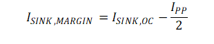
Most modern synchronous buck converters and modules also have a negative current limit or sinking current limit, ISINK,OC. Under no load conditions, the inductor valley current will go negative for devices such as the TPSM5D1806 that operate in forced continuous-conduction mode (FCCM). If too low a switching frequency is used, the steady state inductor current ripple at no load could be large enough that the valley current could exceed the sinking current limit. Thus, a minimum switching frequency is imposed by the sinking current limit. The margin from the sinking current limit is given by Equation 8 and plotted in Figure 4-4 for VIN = 12 V. For a target output voltage, the switching frequency must be selected where there is positive margin from the sinking current limit.
") Figure 4-4 Negative Current Limit Margin
(VIN = 12 V)
Figure 4-4 Negative Current Limit Margin
(VIN = 12 V)The tradeoff of going to higher switching frequency to avoid current limit violations is typically lower efficiency. The TPSM5D1806 data sheet shows the efficiency curves for 12-V input and 1.8-V output at multiple switching frequencies. The 1.8-V efficiency curves for 1 MHz and 1.5 MHz differ at load currents below 3 A, with the 1.5-MHz curve showing lower efficiency owing to higher switching or AC losses than at 1-MHz.
") Figure 4-5 TPSM5D1806
Efficiency vs Output Current (VIN = 12 V)
Figure 4-5 TPSM5D1806
Efficiency vs Output Current (VIN = 12 V)