SLUAAF9 September 2021 UCC28782
- Trademarks
- 1 Initial Board Visual Inspection and Start-up Check
- 2 Typical System Operating Waveforms
- 3Typical System Protection Waveforms
- 4Common Issues and Solutions
- 5References
4.3.1 BIN/BSW Pin Damage During LPM to ABM Mode Transition
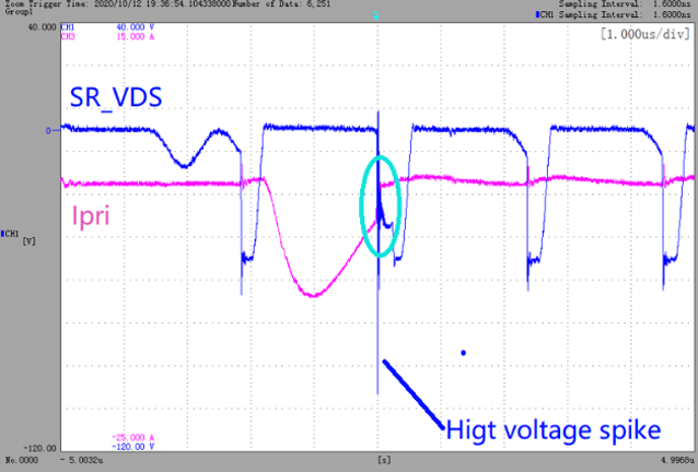
This transition could be caused by RDM or BUR pin resistor not selected properly. When the power stage running at LPM mode, high-side driver PWMH is disabled, transformer leakage energy will be accumulated at clamp capacitors while results in voltage on clamp capacitors slightly higher than output reflected voltage, as load increasing, power stage will transfer from LPM to ABM mode, there is a large balancing current between clamp capacitors and output capacitors when the first PWMH enabled, if PWMH on time is shorten than the resonance time of leakage inductance and clamp capacitors. NON-ZCS turn off will happen as shown in Figure 4-6, A sharp di/dt on leakage inductance causes high voltage spike which coupling to AUX winding, there is a potential risk that damage BIN/BSW pins, and SR FET also shows over voltage stress at this moment.
 Figure 4-6 SR FET Non-ZCS Turn Off
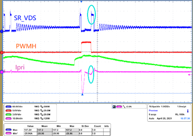
 Figure 4-7 SR FET ZCS Turn Off
Solution:
- Re-calculate RDM pin resistor value,The RRDM calculation equation shown in UCC28782 data sheet equation (11). If the actual value on the tested board is close to calculated value, minor increase RDM resistor until the user can see NON-ZCS turn off disappear, see Figure 4-7
- Decrease down-side resistor value of BUR pin divider. So the peak current at LPM is reduced, in this way, the energy stored in clamp capacitors is also reduced. This process will assist for smaller balancing current.