-
How to Achieve Improved Thermal Performance on TPS56x242-7 with SOT563 Package
How to Achieve Improved Thermal Performance on TPS56x242-7 with SOT563 Package
Trademarks
All trademarks are the property of their respective owners.
1 Introduction
With the development of end equipment (EE), there is a strong trend of smaller size, multifunction, and easy-carry. So high density is more and more important, especially for power. TI released a high-power density part TPS566242/7 which can support 6-A continues current with SOT563 package. SOT563 package body size is only 1.6 × 1.2 mm. Up to now, it is the highest power density part of 16-V/6-A. The challenge of high-power density is thermal performance. This application note introduces how TPS566242/7 solve thermal problems from the device itself and the customer’s board.
2 Improve Thermal Performance from IC Independently
First, from TPS566242/7 independently, it optimizes pin-out definition. Figure 2-1 shows pin-out. The device integrates BST pin and add one AGND for PIN4. This pin-out makes layout very easy on board. Figure 2-1 shows suggested layout. In top layer, it places nearly all line, especially power line as Figure 2-2. It is recommended to connect GND and AGND together to increase GND area to improve thermal performance. FB line goes through on bottom layer to avoid to be affected by switching noise Figure 2-3.
TPS566242/7 integrates small Rdson of 27.7 mohm for high side and 14.8 mohm low side. Small Rdson will cause small conducting loss which will be helpful for high efficiency. And it also increases driving slew rate to reduce switching loss. Below Figure 2-4 and Figure 2-5 show the TPS566242 SW waveform at 12-V Vin to 5-V Vout at 6-A loading. For the rising edge, the slew rate could get 4.25-V/ns. At the same time, this part uses special driver design to decrease switching ring voltage. For the falling edge, the slew rate could get 7.35-V/ns. This fast switching slew rate decreases switching loss which is also helpful for high efficiency.
 Figure 2-4 TPS566242 Rising
Edge
 Figure 2-5 TPS566242 Falling
Edge
Figure 2-5 TPS566242 Falling
Edge3 Improve Thermal Performance from PCB Board
From a customer’s board point, this application note introduces an idea by optimizing layout to improve thermal performance for a small SOT563 package.
PIN 1, 2, and 3 are power pin. It is absolutely important to place large copper area for power line. PIN 4, 5, and 6 are signal pin. Originally signal pin is not necessary to place large copper area. Because it does not go through high current. But for SOT563 package, signal pin is also helpful for heat loss. So large copper area for signal pin is also very helpful for thermal performance. It is recommended to place large copper area for signal pin. Because SOT563 package is small and die size is also small. There is thermal radiation path from FETs area to the signal area because the path is very shot short, so the thermal is able to be dissipated to the signal pins. And TPS566242/7 uses FCOL(Flip Chip On Lead) technology. The copper bump is very helpful for heat conduction from die to pin. Large signal pin copper area can quickly make thermal transfer to PCB board and ambient. The biggest part of thermal is still transferred from FET area. Figure 3-1 shows thermal transfer path.
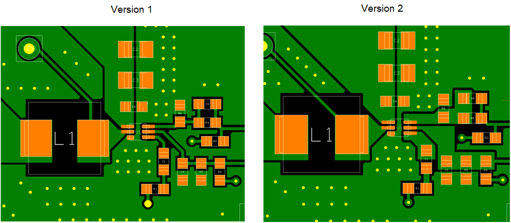
Following are two types of EVM boards which are made to compare the thermal performance. Figure 3-2 version 1 shows one EVM layout in which signal line is normal width with 20-mil. Version 2 shows another EVM layout in which signal line is large copper area.
 Figure 3-2 PCB Board with Two Version Types
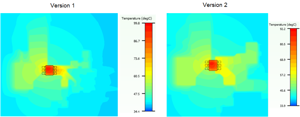
First thermal information is simulated by Ansys software. Figure 3-3 shows the simulation result at same simulation conditions. The highest temp is lower than in version 2. And compare signal pin temperature, the version 1 temperature is higher than second figure which means heat could not quickly transfer to ambient. In version 2, the signal pin area is lower because large signal copper area can make heat quickly transfer to PCB board and ambient.
 Figure 3-3 Simulation Result with Two Versions
Test result with same conditions on PCB board by camera is shown in Figure 3-4. From test results, the thermal of version 1 is higher than version 2. And the signal pin area of version 1 is also higher than version 2.
4 Thermal Performance
This topic introduces thermal performance of this EVM family.
Figure 4-1, Figure 4-2, and Figure 4-3 show TPS566242 thermal performance at different conditions. TPS566242 public EVM board is used to test. This EVM board has 4-layers which includes 2 internal layers with 1-oz copper and top, bottom layer with 2-oz copper. Test ambient temp is room temp.
Figure 4-4, Figure 4-5, and Figure 4-6 show TPS565242 thermal performance at different conditions. TPS565242 public EVM board is used to test. This EVM board has 2-layers in which top and bottom layers are 2-oz copper.
Figure 4-7, Figure 4-8, and Figure 4-9 show TPS564242 thermal performance at different conditions. TPS564242 public EVM board is used to test. This EVM board has 2-layesr in which top and bottom layers are 2-oz copper.
Table 4-1 shows a summary of this efficiency and thermal performance.
| Part number | Vin/V | Vout/V | Iout/A | Efficiency | Temperature |
|---|---|---|---|---|---|
| TPS566242 | 12 | 1.05 | 6 | 82.38% | 80 |
| TPS566242 | 12 | 3.3 | 6 | 91.67% | 91 |
| TPS566242 | 12 | 5 | 6 | 93.75% | 97 |
| TPS565242 | 12 | 1.05 | 5 | 83.94% | 72 |
| TPS565247 | 12 | 3.3 | 5 | 92.86% | 81 |
| TPS565247 | 12 | 5 | 5 | 94.63% | 86 |
| TPS564242 | 12 | 1.05 | 4 | 83.61% | 64 |
| TPS564242 | 12 | 3.3 | 4 | 93.50% | 73 |
| TPS564242 | 12 | 5 | 4 | 95.41% | 75 |