SLUAAJ5 April 2022 TPS565242 , TPS565247 , TPS566242 , TPS566247
3 Improve Thermal Performance from PCB Board
From a customer’s board point, this application note introduces an idea by optimizing layout to improve thermal performance for a small SOT563 package.
PIN 1, 2, and 3 are power pin. It is absolutely important to place large copper area for power line. PIN 4, 5, and 6 are signal pin. Originally signal pin is not necessary to place large copper area. Because it does not go through high current. But for SOT563 package, signal pin is also helpful for heat loss. So large copper area for signal pin is also very helpful for thermal performance. It is recommended to place large copper area for signal pin. Because SOT563 package is small and die size is also small. There is thermal radiation path from FETs area to the signal area because the path is very shot short, so the thermal is able to be dissipated to the signal pins. And TPS566242/7 uses FCOL(Flip Chip On Lead) technology. The copper bump is very helpful for heat conduction from die to pin. Large signal pin copper area can quickly make thermal transfer to PCB board and ambient. The biggest part of thermal is still transferred from FET area. Figure 3-1 shows thermal transfer path.
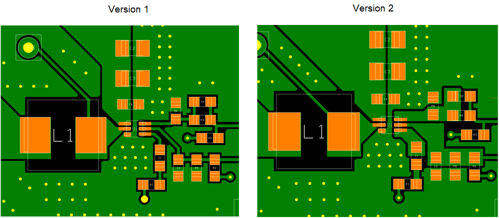
Following are two types of EVM boards which are made to compare the thermal performance. Figure 3-2 version 1 shows one EVM layout in which signal line is normal width with 20-mil. Version 2 shows another EVM layout in which signal line is large copper area.
 Figure 3-2 PCB Board with Two Version Types
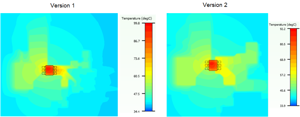
First thermal information is simulated by Ansys software. Figure 3-3 shows the simulation result at same simulation conditions. The highest temp is lower than in version 2. And compare signal pin temperature, the version 1 temperature is higher than second figure which means heat could not quickly transfer to ambient. In version 2, the signal pin area is lower because large signal copper area can make heat quickly transfer to PCB board and ambient.
 Figure 3-3 Simulation Result with Two Versions
Test result with same conditions on PCB board by camera is shown in Figure 3-4. From test results, the thermal of version 1 is higher than version 2. And the signal pin area of version 1 is also higher than version 2.