SLUAAM4 December   2023 BQ76905 , BQ76907


  1.   1
  2.   Abstract
  3.   Trademarks
  4. 1Direct Commands
    1. 1.1 Alarm Enable - 0x66
    2. 1.2 Cell 1 Voltage - 0x14
    3. 1.3 Internal Temperature - 0x28
    4. 1.4 CC2 Current - 0x3A
    5. 1.5 Direct Command Summary
      1. 1.5.1 Disabling Auto Refresh
  5. 2Subcommands
    1. 2.1 DEVICE_NUMBER - 0x0001
    2. 2.2 FET_ENABLE - 0x0022
    3. 2.3 RESET - 0x0012
    4. 2.4 CB_ACTIVE_CELLS - 0x0083
    5. 2.5 Subcommand Summary
  6. 3Reading and Writing RAM Registers
    1. 3.1 Read Enabled Protections A
    2. 3.2 Enter CONFIG_UPDATE Mode
    3. 3.3 Write Enabled Protections A
    4. 3.4 Write VCell Mode
    5. 3.5 Exit CONFIG_UPDATE Mode
    6. 3.6 Reading and Writing RAM Registers Summary
  7. 4I2C With CRC
  8. 5Simple Code Examples
  9. 6References

Write Enabled Protections A

In this example, the CUV (undervoltage) protection feature is enabled along with the default protections. This requires writing 0xE1 to RAM address 0x9024, shown in Figure 3-3. The checksum is calculated on the address and data (0x24, 0x90, 0xE1) and is the complement of the sum of these bytes. In this case, the checksum is 0x6A. The length includes the two bytes for device address and command address for a total length of 0x05.
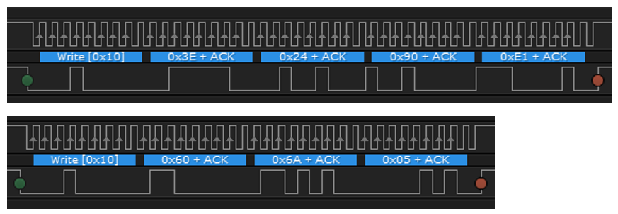
GUID-20220822-SS0I-4GQJ-5JM7-XLX15GFVGCZB-low.pngFigure 3-3 Captured Waveform for Writing to Enabled Protections A