SLUAAP7 January 2024 BQ76905 , BQ76907
2.1 Internal Cell-Balancing Circuit Design
When one of the internal balance FETs is enabled, the internal FET will pull the pins for that cell together drawing current through the input resistors for that cell. The recommended minimum value of the input filter resistors when using internal balancing is 20Ω. This value maximizes the balance current while keeping it well within the absolute maximum cell balancing current over the internal FET RDS(ON) range. The maximum recommended value for the input filter resistors is 1kΩ.
The typical internal cell balancing resistance (RDS(ON) for the internal FET) is 80Ω. For a typical lithium ion cell with a full charge voltage of 4.2V, this results in a balancing current of approximately 35mA. This is the DC current assuming the switch was continuously on; therefore, the average balancing current will be lower. The duty cycle is determined by a multiple factors which are discussed in more detail in Section 4.
 Figure 2-1 Application Circuit for Internal Balancing
For many applications, the internal balancing current for the device is sufficient and additional external components are not required. However, one must consider the power dissipation and the resulting impact on the device temperature. For example, 35mA into 80Ω results in about 0.098W (almost 100-mW). The junction to ambient thermal resistance (θ-JA) for the device is 47.2 °C/W. If 5-cells are balancing at the same time, this can result in a junction temperature rise of approximately 23 °C.
There are different alternatives to mitigate excessive power dissipation. The host can limit the maximum number of cells allowed to balance simultaneously, refer to How to Limit Maximum Balancing Cells. Another alliterative is to increase the cell input resistors, in order to reduce the balancing current and improve power dissipation.
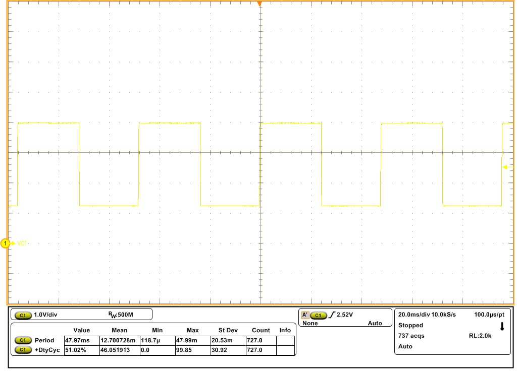
 Figure 2-2 Internal Cell Balancing on
Cell 1 (VC1)