SLUS774C AUGUST 2007 – December 2014 TPS54383 , TPS54386
PRODUCTION DATA.
- 1 Features
- 2 Applications
- 3 Description
- 4 Revision History
- 5 Pin Configuration and Functions
- 6 Specifications
-
7 Detailed Description
- 7.1 Overview
- 7.2 Functional Block Diagram
- 7.3
Feature Description
- 7.3.1 Voltage Reference
- 7.3.2 Oscillator
- 7.3.3 Input Undervoltage Lockout (UVLO) and Startup
- 7.3.4 Enable and Timed Turn On of the Outputs
- 7.3.5 Output Voltage Sequencing
- 7.3.6 Soft-Start
- 7.3.7 Output Voltage Regulation
- 7.3.8 Feedback Loop and Inductor-Capacitor (L-C) Filter Selection
- 7.3.9 Inductor-Capacitor (L-C) Selection
- 7.3.10 Maximum Output Capacitance
- 7.3.11 Minimum Output Capacitance
- 7.3.12 Modifying The Feedback Loop
- 7.3.13 Example: TPS54386 Buck Converter Operating at 12-V Input, 3.3-V Output and 400-mA(P-P) Ripple Current
- 7.3.14 Bootstrap for the N-Channel MOSFET
- 7.3.15 Light Load Operation
- 7.3.16 SW Node Ringing
- 7.3.17 Output Overload Protection
- 7.3.18 Operating Near Maximum Duty Cycle
- 7.3.19 Dual Supply Operation
- 7.3.20 Cascading Supply Operation
- 7.3.21 Multiphase Operation
- 7.3.22 Bypass and FIltering
- 7.3.23 Overtemperature Protection and Junction Temperature Rise
- 7.3.24 Power Derating
- 7.4 Device Functional Modes
-
8 Applications and Implementation
- 8.1 Application Information
- 8.2
Typical Applications
- 8.2.1
12-V to 5-V and 3.3-V Converter
- 8.2.1.1 Design Requirements
- 8.2.1.2
Detailed Design Procedure
- 8.2.1.2.1 Duty Cycle Estimation
- 8.2.1.2.2 Inductor Selection
- 8.2.1.2.3 Rectifier Diode Selection
- 8.2.1.2.4 Output Capacitor Selection
- 8.2.1.2.5 Voltage Setting
- 8.2.1.2.6 Compensation Capacitors
- 8.2.1.2.7 Input Capacitor Selection
- 8.2.1.2.8 Boot Strap Capacitor
- 8.2.1.2.9 ILIM
- 8.2.1.2.10 SEQ
- 8.2.1.2.11 Power Dissipation
- 8.2.1.3 Application Curves
- 8.2.2 24-V to 12-V and 24-V to 5-V
- 8.2.3 5-V to 3.3V and 5-V to 1.2 V
- 8.2.1
12-V to 5-V and 3.3-V Converter
- 9 Power Supply Recommendations
- 10Layout
- 11Device and Documentation Support
- 12Mechanical, Packaging, and Orderable Information
1 Features
- 4.5-V to 28-V Input Range
- Output Voltage Range 0.8 V to 90% of Input Voltage
- Output Current Up to 3 A
- Two Fixed Switching Frequency Versions:
- TPS54383: 300 kHz
- TPS54386: 600 kHz
- Three Selectable Levels of Overcurrent Protection (Output 2)
- 0.8-V 1.5% Voltage Reference
- 2.1-ms Internal Soft-Start
- Dual PWM Outputs 180° Out-of-Phase
- Ratiometric or Sequential Startup Modes Selectable by a Single Pin
- 85-mΩ Internal High-Side MOSFETs
- Current Mode Control
- Internal Compensation (See Page 16)
- Pulse-by-Pulse Overcurrent Protection
- Thermal Shutdown Protection at +148°C
- 14-Pin PowerPAD™ HTSSOP package
2 Applications
- Set Top Box
- Digital TV
- Power for DSP
- Consumer Electronics
3 Description
The TPS54383 and TPS54386 are dual output, non-synchronous buck converters capable of supporting 3-A output applications that operate from a 4.5-V to 28-V input supply voltage, and require output voltages between 0.8 V and 90% of the input voltage.
With an internally-determined operating frequency, soft-start time, and control loop compensation, these converters provide many features with a minimum of external components. Channel 1 overcurrent protection is set at 4.5 A, while Channel 2 overcurrent protection level is selected by connecting a pin to ground, to BP, or left floating. The setting levels are used to allow for scaling of external components for applications that do not need the full load capability of both outputs.
The outputs may be enabled independently, or may be configured to allow either ratio-metric or sequential startup sequencing. Additionally, the two outputs may be powered from different sources.
Device Information(1)
| PART NUMBER | PACKAGE | BODY SIZE (NOM) |
|---|---|---|
| TPS54383 | HTSSOP (14) | 4.40 mm × 5.00 mm |
| TPS54386 |
- For all available packages, see the orderable addendum at the end of the datasheet.
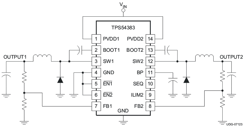
Simplified Schematic
4 Revision History
Changes from B Revision (October 2007) to C Revision
- Added ESD Ratings table, Feature Description section, Device Functional Modes, Application and Implementation section, Power Supply Recommendations section, Layout section, Device and Documentation Support section, and Mechanical, Packaging, and Orderable Information section.Go