SLUS825C February 2008 – August 2014 TPS53124
PRODUCTION DATA.
- 1Simplified Schematics
- 2Pin Configuration and Functions
- 3Specifications
- 4Detailed Description
-
5Application and Implementation
- 5.1 Application Information
- 5.2
Typical Application
- 5.2.1 Design Requirements
- 5.2.2
Detailed Design Procedure
- 5.2.2.1 Choose Inductor
- 5.2.2.2 Loop Compensation and External Parts Selection
- 5.2.2.3 Choose Input Capacitor
- 5.2.2.4 Choose Bootstrap Capacitor
- 5.2.2.5 Choose VREG5 and V5FILT Capacitor
- 5.2.2.6 Choose Output Voltage Set Point Resistors
- 5.2.2.7 Choose Over Current Set Point Resistor
- 5.2.2.8 Choose Soft Start Capacitor
- 5.2.3 Application Curves (QFN)
- 6Power Supply Recommendations
- 7Layout
5 Application and Implementation
5.1 Application Information
The TPS53124 is a dual, Adaptive on-time DCAP™ mode synchronous controller. The part enables system designers to cost effectively complete the suite of digital TV power bus regulators with the absolute lowest external component count and lowest standby consumption. The main control loop for the TPS53124 uses the D-CAP™ mode that optimized for low ESR output capacitors such as POSCAP or SP-CAP promises fast transient response with no external compensation. The part provides a convenient and efficient operation with conversion voltages from 4.5 V to 24 V and output voltage from 0.76 V to 5.5 V.
5.2 Typical Application
The TPS53124 is a Step-Down Controller in a realistic cost-sensitive application. Providing both a low core-type 1.05 V and I/O type 1.8 V output from a loosely regulated 12 V source. Idea applications are: Digital TV Power Supply, Networking Home Pin and Digital Set-Top Box (STB).
 Figure 6. TPS53124 Typical Application Circuit (QFN)
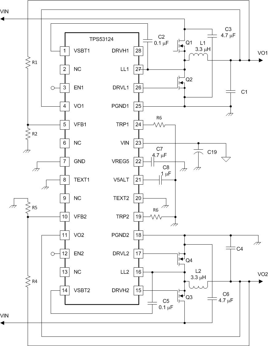 Figure 7. TSSOP
5.2.1 Design Requirements
Table 1. Design Parameters
| PARAMETERS | EXAMPLE VALUES |
|---|---|
| Input voltage | 12 V |
| Output voltage | VO1 = 1.8 V, VO2 = 1.05 V |
5.2.2 Detailed Design Procedure
5.2.2.1 Choose Inductor
The inductance value is selected to provide approximately 30% peak to peak ripple current at maximum load. Larger ripple current increases output ripple voltage, improve S/N ratio and contribute to stable operation.
Equation 3 can be used to calculate L1.

The inductors current ratings needs to support both the RMS (thermal) current and the Peak (saturation) current. The RMS and peak inductor current can be estimated as follows.


NOTE
The calculation above shall serve as a general reference. To further improve transient response, the output inductance could be reduced further. This needs to be considered along with the selection of the output capacitor.
5.2.2.2 Loop Compensation and External Parts Selection
A buck converter system using D-CAP™ Mode can be simplified as below.
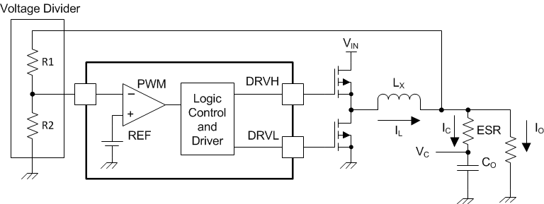 Figure 8. Simplifying the Modulator
The output voltage is compared with internal reference voltage after divider resistors, R1 and R2. The PWM comparator determines the timing to turn on top MOSFET. The gain and speed of the comparator is high enough to keep the voltage at the beginning of each on cycle (or the end of off cycle) substantially constant. The DC output voltage may have line regulation due to ripple amplitude that slightly increases as the input voltage increase.
For the loop stability, the 0-dB frequency, f0, defined below need to be lower than 1/3 of the switching frequency.

Although D-CAP™ Mode provides many advantages such as ease-of-use, minimum external components configuration and extremely short response time, a sufficient amount of feedback signal needs to be provided by external circuit to reduce jitter level. This is due to not employing an error amplifier in the loop. The required signal level is approximately 10 mV at the comparing point (VFB terminal). This gives Vripples at the output node becomes Equation 8.The output capacitor’s ESR should meet this requirement.

5.2.2.3 Choose Input Capacitor
The TPS53124 requires an input decoupling capacitor and a bulk capacitor is needed depending on the application. A minimum 10-μF high-quality ceramic capacitor is recommended for the input capacitor. The capacitor voltage rating needs to be greater than the maximum input voltage.
5.2.2.4 Choose Bootstrap Capacitor
The TPS53124 requires a bootstrap capacitor from SW to VBST to provide the floating supply for the high-side drivers. A minimum 0.1-μF high-quality ceramic capacitor is recommended. The voltage rating should be greater than 10 V.
5.2.2.5 Choose VREG5 and V5FILT Capacitor
The TPS53124 requires both the VREG5 regulator and V5FILT input are bypassed. A minimum 4.7-μF high-quality ceramic capacitor must be connected between the VREG5 and GND for proper operation. A minimum 1-μF high-quality ceramic capacitor must be connected between the V5FILT and GND for proper operation. Both of these capacitors’ voltage ratings should be greater than 10 V.
5.2.2.6 Choose Output Voltage Set Point Resistors
The output voltage is set with a resistor divider from the output voltage node to the VFBx pin. It is recommended to use 1% tolerance or better resisters. Select R2 between 10 kΩ and 100 kΩ and use Equation 9 or Equation 10 to calculate R1.


Where
VFB(RIPPLE) = Ripple voltage at VFB
Vswinj = Ripple voltage at error comparator
5.2.2.7 Choose Over Current Set Point Resistor


Where
RDS(ON) = Low-side FET on-resistance
ITRIP(min) = TRIP pin source current (8.5 μA)
VOCL0ff = Minimum over current limit offset voltage (–20 mV)
IOCL = Over current limit
5.2.2.8 Choose Soft Start Capacitor
Soft-start time equation is as follows.

5.2.3 Application Curves (QFN)
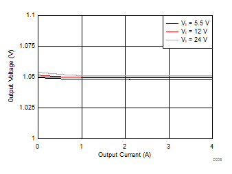 Figure 9. CH1 Output Voltage vs Output Current
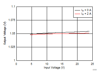 Figure 11. CH1 Output Voltage vs Input Voltage
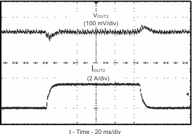 Figure 13. CH1 Load Step Response
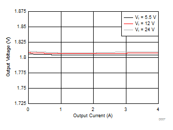 Figure 10. CH2 Output Voltage vs Output Current
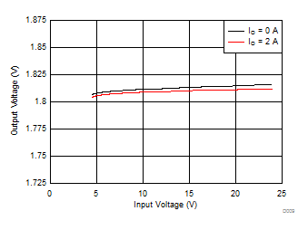 Figure 12. CH2 Output Voltage vs Input Voltage
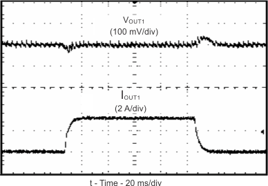 Figure 14. CH2 Load Step Response