-
UCC27211 120V, 3.7A/4.5A Half-Bridge Driver with 8V UVLO
- 1
- 1 Features
- 2 Applications
- 3 Description
- 4 Pin Configuration and Functions
- 5 Specifications
- 6 Detailed Description
- 7 Application and Implementation
- 8 Power Supply Recommendations
- 9 Layout
- 10Device and Documentation Support
- 11Revision History
- 12Mechanical, Packaging, and Orderable Information
- IMPORTANT NOTICE
UCC27211 120V, 3.7A/4.5A Half-Bridge Driver with 8V UVLO
1 Features
- Drives two N-channel MOSFETs in high-side and low-side configuration with independent inputs
- Maximum boot voltage 120V DC
- 3.7A source, 4.5A sink output currents
- Input pins can tolerate –10V to 20V and are independent of supply voltage range
- TTL compatible input versions
- 8V to 17V VDD operating range, (20V absolute maximum)
- 7.2ns rise and 5.5ns fall time with 1000pF load
- Fast propagation delay times (20ns typical)
- 4ns delay matching
- Symmetrical undervoltage lockout for high-side and low-side driver
- All industry standard packages available (SOIC-8, PowerPAD™ SOIC-8, 4mm × 4mm SON-8 and 4mm × 4mm SON-10)
- Specified from –40°C to 150°C
2 Applications
- Solar power optimizers and micro inverters
- Telecom and merchant power supplies
- Online and offline UPS
- Energy storage systems
- Battery test equipment
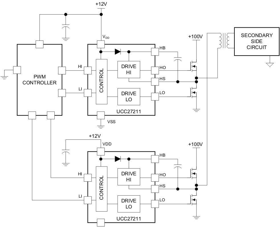
 Typical Application
3 Description
The UCC27211 driver is based on the popular UCC27201 MOSFET drivers, but offer several significant performance improvements. Peak output pull-up and pull-down current has been increased to 3.7A source and 4.5A sink, thereby allowing for driving large power MOSFETs with minimized switching losses during the transition through the Miller Plateau of the MOSFET. The input structure is now able to directly handle –10VDC, which increases robustness and also allows direct interface to gate-drive transformers without using rectification diodes. The inputs are also independent of supply voltage and have a maximum rating of 20V.
The switching node (HS pin) can handle –(24 – VDD) V maximum which allows the high-side channel to be protected from inherent negative voltages caused parasitic inductance and stray capacitance. UCC27211 (TTL inputs) has increased input hysteresis allowing for interface to analog or digital PWM controllers with enhanced noise immunity.
The low-side and high-side gate drivers are independently controlled and matched to 4 ns between the turnon and turnoff of each other. An on-chip 120V rated bootstrap diode eliminates the external discrete diodes.
Undervoltage lockout is provided for both the high-side and the low-side drivers providing symmetric turnon and turnoff behavior and forcing the outputs low if the drive voltage is below the specified threshold.
| PART NUMBER | PACKAGE | BODY SIZE (NOM) |
|---|---|---|
| UCC27211 | D (SOIC 8) | 4.9mm × 3.9mm |
| DDA (PowerPAD 8) | 4.9mm × 3.9mm | |
| DPR (WSON 10) | 4.0mm × 4.0mm | |
| DRM (VSON 8) |