SLUSCE9B
June 2017 – March 2020
UCC27712
PRODUCTION DATA.
1
Features
2
Applications
3
Description
Device Images
Simplified Schematic
Typical Propagation Delay Comparison
4
Revision History
5
Pin Configuration and Functions
Pin Functions
6
Specifications
6.1
Absolute Maximum Ratings
6.2
ESD Ratings
6.3
Recommended Operating Conditions
6.4
Thermal Information
6.5
Electrical Characteristics
6.6
Dynamic Electrical Characteristics
6.7
Typical Characteristics
7
Detailed Description
7.1
Overview
7.2
Functional Block Diagram
7.3
Feature Description
7.3.1
VDD and Under Voltage Lockout
7.3.2
Input and Output Logic Table
7.3.3
Input Stage
7.3.4
Output Stage
7.3.5
Level Shift
7.3.6
Low Propagation Delays and Tightly Matched Outputs
7.3.7
Parasitic Diode Structure
7.4
Device Functional Modes
7.4.1
Minimum Input Pulse Operation
7.4.2
Output Interlock and Dead Time
7.4.3
Operation Under 100% Duty Cycle Condition
7.4.4
Operation Under Negative HS Voltage Condition
8
Application and Implementation
8.1
Application Information
8.2
Typical Application
8.2.1
Design Requirements
8.2.2
Detailed Design Procedure
8.2.2.1
Selecting HI and LI Low Pass Filter Components (RHI, RLI, CHI, CLI)
8.2.2.2
Selecting Bootstrap Capacitor (CBOOT)
8.2.2.3
Selecting VDD Bypass/Holdup Capacitor (CVDD) and Rbias
8.2.2.4
Selecting Bootstrap Resistor (RBOOT)
8.2.2.5
Selecting Gate Resistor RON/ROFF
8.2.2.6
Selecting Bootstrap Diode
8.2.2.7
Estimate the UCC27712 Power Losses (PUCC27712)
8.2.2.8
Estimating Junction Temperature
8.2.2.9
Operation With IGBT's
8.2.3
Application Curves
9
Power Supply Recommendations
10
Layout
10.1
Layout Guidelines
10.2
Layout Example
11
Device and Documentation Support
11.1
Documentation Support
11.1.1
Related Documentation
11.2
Related Links
11.3
Community Resources
11.4
Trademarks
11.5
Electrostatic Discharge Caution
11.6
Glossary
12
Mechanical, Packaging, and Orderable Information
6.7
Typical Characteristics
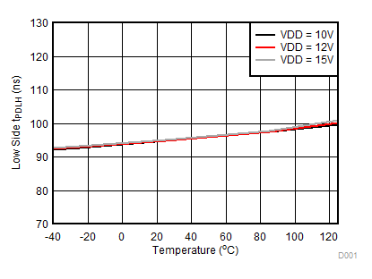
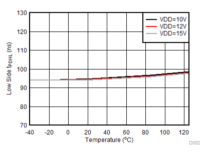
Figure 2.
Low-Side, Turn-On Propagation Delay vs Temperature
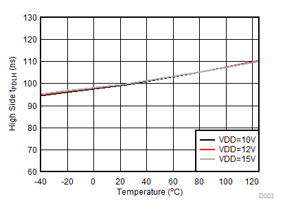
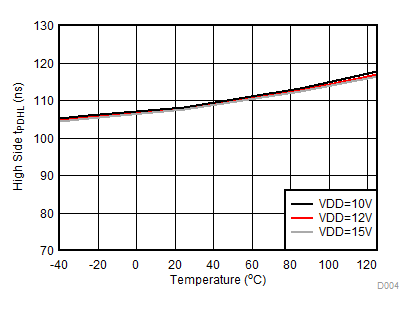
Figure 4.
High-Side, Turn-On Propagation Delay vs Temperature
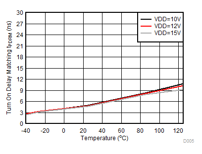
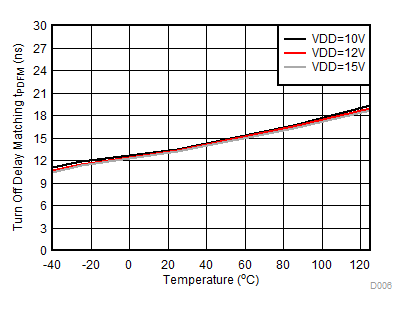
Figure 6.
Turn-On Delay Matching vs Temperature
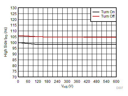
Figure 8.
High-Side Propagation Delay vs HS
Figure 10.
LO Fall Time with 1000-pF Load vs Temperature
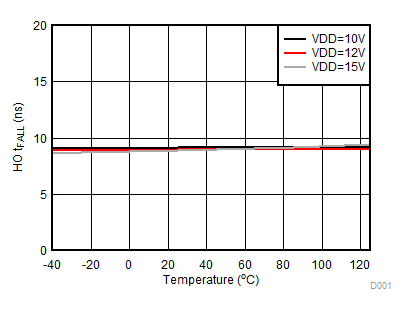
Figure 12.
HO Fall Time with 1000-pF Load vs Temperature
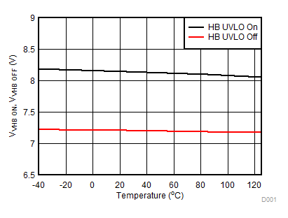
Figure 14.
VHB-VHS UVLO Thresholds vs Temperature
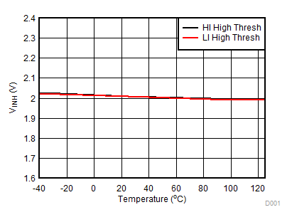
Figure 16.
HI/LI Pin High Threshold vs Temperature
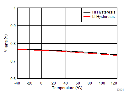
Figure 18.
HI/LI Pin Hysteresis vs Temperature
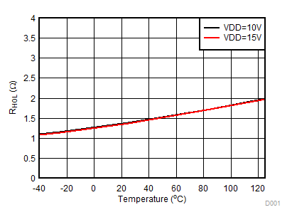
Figure 20.
HO Output Pull-Down Resistance vs Temperature
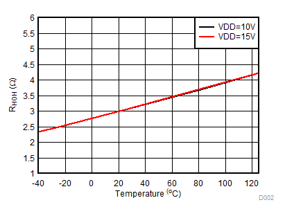
Figure 22.
HO Output Pull-Up Resistance vs Temperature
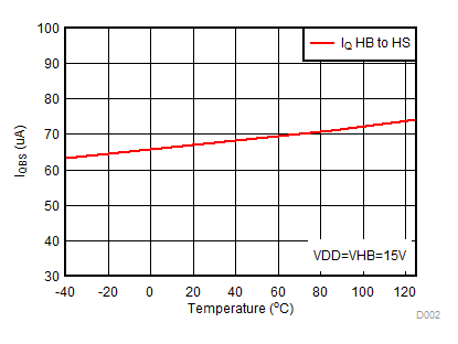
Figure 24.
Quiescent HB to HS Supply Current vs Temperature
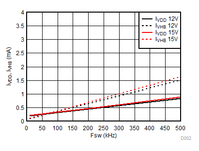
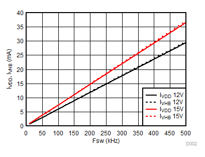
Figure 26.
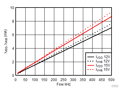
VDD and HB Operating Current with No Load vs Switching Frequency
Figure 28.
VDD and HB Operating Current with 4700-pF Load vs Switching Frequency
Figure 3.
Low-Side, Turn-Off Propagation Delay vs Temperature
Figure 5.
High-Side, Turn-Off Propagation Delay vs Temperature
Figure 7.
Turn-Off Delay Matching vs Temperature
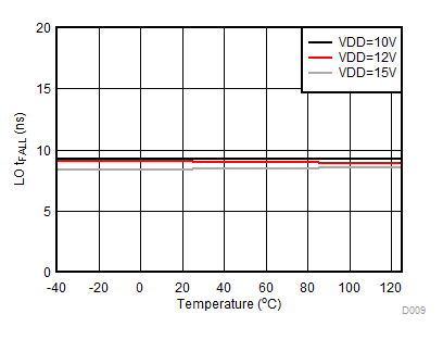
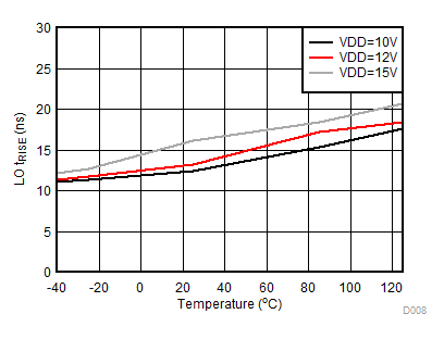
Figure 9.
LO Rise Time with 1000-pF Load vs Temperature
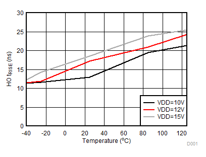
Figure 11.
HO Rise Time with 1000-pF Load vs Temperature
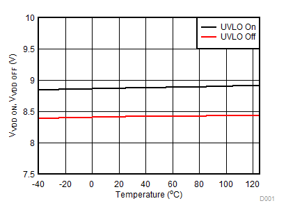
Figure 13.
VDD UVLO Thresholds vs Temperature
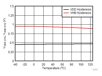
Figure 15.
VDD and VHB-VHS UVLO Hysteresis vs Temperature
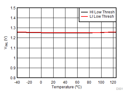
Figure 17.
HI/LI Pin Low Threshold vs Temperature
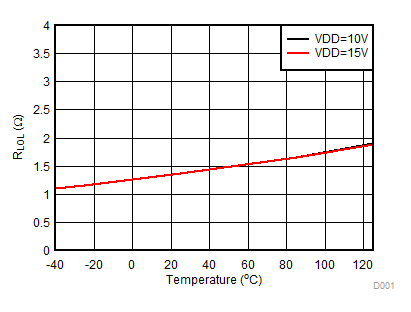
Figure 19.
LO Output Pull-Down Resistance vs Temperature
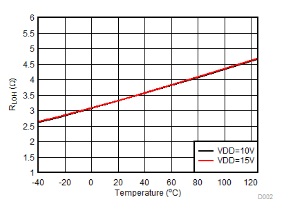
Figure 21.
LO Output Pull-Up Resistance vs Temperature
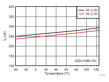
Figure 23.
Total Quiescent VDD plus HB Supply Current vs Temperature
Figure 25.
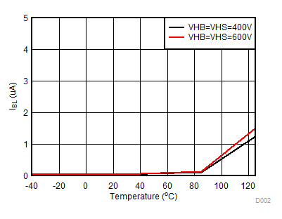
HB to COM Bootstrap Supply Leakage Current vs Temperature
Figure 27.
VDD and HB Operating Current with 1000-pF Load vs Switching Frequency