SLUSCO9A
September 2016 – October 2016
TPS254900-Q1
PRODUCTION DATA.
1
Features
2
Applications
3
Description
4
Revision History
5
Pin Configuration and Functions
6
Specifications
6.1
Absolute Maximum Ratings
6.2
ESD Ratings
6.3
Recommended Operating Conditions
6.4
Thermal Information
6.5
Electrical Characteristics
6.6
Switching Characteristics
6.7
Typical Characteristics
7
Parameter Measurement Information
8
Detailed Description
8.1
Overview
8.2
Functional Block Diagram
8.3
Feature Description
8.3.1
FAULT Response
8.3.2
Cable Compensation
8.3.2.1
Design Procedure
8.3.3
D+ and D- Protection
8.3.4
VBUS OVP Protection
8.3.5
Output and D+ or D- Discharge
8.3.6
Port Power Management (PPM)
8.3.6.1
Benefits of PPM
8.3.6.2
PPM Details
8.3.6.3
Implementing PPM in a System With Two Charging Ports (CDP and SDP1)
8.3.7
Overcurrent Protection
8.3.8
Undervoltage Lockout
8.3.9
Thermal Sensing
8.3.10
Current-Limit Setting
8.4
Device Functional Modes
8.4.1
Device Truth Table (TT)
8.4.2
USB BC1.2 Specification Overview
8.4.3
Standard Downstream Port (SDP) Mode — USB 2.0 and USB 3.0
8.4.4
Charging Downstream Port (CDP) Mode
8.4.5
Client Mode
8.4.6
High-Bandwidth Data-Line Switch
9
Application and Implementation
9.1
Application Information
9.2
Typical Application
9.2.1
Design Requirements
9.2.2
Detailed Design Procedure
9.2.2.1
Input Capacitance
9.2.2.2
Output Capacitance
9.2.2.3
BIAS Capacitance
9.2.2.4
Output and BIAS TVS
9.2.3
Application Curves
10
Power Supply Recommendations
11
Layout
11.1
Layout Guidelines
11.2
Layout Example
12
Device and Documentation Support
12.1
Device Support
12.1.1
Third-Party Products Disclaimer
12.2
Documentation Support
12.2.1
Related Documentation
12.3
Receiving Notification of Documentation Updates
12.4
Community Resources
12.5
Trademarks
12.6
Electrostatic Discharge Caution
12.7
Glossary
13
Mechanical, Packaging, and Orderable Information
7 Parameter Measurement Information
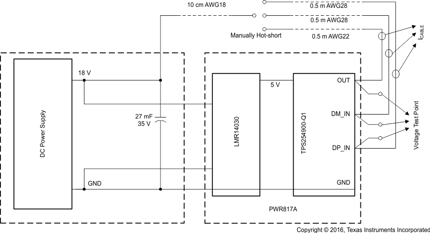
Figure 36. Short-to-Battery System Test Setup