SLUSDG1C June   2020  ā€“ August 2022 BQ25792

PRODUCTION DATA  

  1. Features
  2. Applications
  3. Description
  4. Revision History
  5. Device Comparison
  6. Description (continued)
  7. Pin Configuration and Functions
  8. Specifications
    1. 8.1 Absolute Maximum Ratings
    2. 8.2 ESD Ratings
    3. 8.3 Recommended Operating Conditions
    4. 8.4 Thermal Information
    5. 8.5 Electrical Characteristics
    6. 8.6 Timing Requirements
    7. 8.7 Typical Characteristics
  9. Detailed Description
    1. 9.1 Overview
    2. 9.2 Functional Block Diagram
    3. 9.3 Feature Description
      1. 9.3.1  Device Power-On-Reset
      2. 9.3.2  PROG Pin Configuration
      3. 9.3.3  Device Power Up from Battery without Input Source
      4. 9.3.4  Device Power Up from Input Source
        1. 9.3.4.1 Power Up REGN LDO
        2. 9.3.4.2 Poor Source Qualification
        3. 9.3.4.3 ILIM_HIZ Pin
        4. 9.3.4.4 Default VINDPM Setting
        5. 9.3.4.5 Input Source Type Detection
          1. 9.3.4.5.1 D+/Dā€“ Detection Sets Input Current Limit
          2. 9.3.4.5.2 HVDCP Detection Procedure
          3. 9.3.4.5.3 Connector Fault Detection
      5. 9.3.5  Dual-Input Power Mux
        1. 9.3.5.1 ACDRV Turn On Condition
        2. 9.3.5.2 VBUS Input Only
        3. 9.3.5.3 One ACFET-RBFET
        4. 9.3.5.4 Two ACFETs-RBFETs
      6. 9.3.6  Buck-Boost Converter Operation
        1. 9.3.6.1 Force Input Current Limit Detection
        2. 9.3.6.2 Input Current Optimizer (ICO)
        3. 9.3.6.3 Pulse Frequency Modulation (PFM)
        4. 9.3.6.4 Device HIZ State
      7. 9.3.7  USB On-The-Go (OTG)
        1. 9.3.7.1 OTG Mode to Power External Devices
      8. 9.3.8  Power Path Management
        1. 9.3.8.1 Narrow VDC Architecture
        2. 9.3.8.2 Dynamic Power Management
      9. 9.3.9  Battery Charging Management
        1. 9.3.9.1 Autonomous Charging Cycle
        2. 9.3.9.2 Battery Charging Profile
        3. 9.3.9.3 Charging Termination
        4. 9.3.9.4 Charging Safety Timer
        5. 9.3.9.5 Thermistor Qualification
          1. 9.3.9.5.1 JEITA Guideline Compliance in Charge Mode
          2. 9.3.9.5.2 Cold/Hot Temperature Window in OTG Mode
      10. 9.3.10 Integrated 16-Bit ADC for Monitoring
      11. 9.3.11 Status Outputs ( STAT, and INT)
        1. 9.3.11.1 Charging Status Indicator (STAT Pin)
        2. 9.3.11.2 Interrupt to Host ( INT)
      12. 9.3.12 Ship FET Control
        1. 9.3.12.1 Shutdown Mode
        2. 9.3.12.2 Ship Mode
        3. 9.3.12.3 System Power Reset
      13. 9.3.13 Protections
        1. 9.3.13.1 Voltage and Current Monitoring
        2. 9.3.13.2 Thermal Regulation and Thermal Shutdown
      14. 9.3.14 Serial Interface
        1. 9.3.14.1 Data Validity
        2. 9.3.14.2 START and STOP Conditions
        3. 9.3.14.3 Byte Format
        4. 9.3.14.4 Acknowledge (ACK) and Not Acknowledge (NACK)
        5. 9.3.14.5 Target Address and Data Direction Bit
        6. 9.3.14.6 Single Write and Read
        7. 9.3.14.7 Multi-Write and Multi-Read
    4. 9.4 Device Functional Modes
      1. 9.4.1 Host Mode and Default Mode
      2. 9.4.2 Register Bit Reset
    5. 9.5 Register Map
      1. 9.5.1 I2C Registers
  10. 10Application and Implementation
    1. 10.1 Application Information
    2. 10.2 Typical Application
      1. 10.2.1 Design Requirements
      2. 10.2.2 Detailed Design Procedure
        1. 10.2.2.1 Inductor Selection
        2. 10.2.2.2 Input (VBUS / PMID) Capacitor
        3. 10.2.2.3 Output (VSYS) Capacitor
      3. 10.2.3 Application Curves
  11. 11Power Supply Recommendations
  12. 12Layout
    1. 12.1 Layout Guidelines
    2. 12.2 Layout Example
  13. 13Device and Documentation Support
    1. 13.1 Device Support
      1. 13.1.1 Third-Party Products Disclaimer
    2. 13.2 Documentation Support
      1. 13.2.1 Related Documentation
    3. 13.3 Receiving Notification of Documentation Updates
    4. 13.4 Support Resources
    5. 13.5 Trademarks
    6. 13.6 Electrostatic Discharge Caution
    7. 13.7 Glossary
  14. 14Mechanical, Packaging, and Orderable Information

Narrow VDC Architecture

The device deploys Narrow VDC architecture (NVDC) with BATFET separating system from battery. The minimum system voltage is set by VSYSMIN bits. Even with a fully depleted battery, the system is regulated above the minimum system voltage. The default minimum system voltage at POR is determined according to the PROG pin configuration resistor.

The NVDC architecture also provides charging termination when the battery is fully charged. By turning off the BATFET, the adapter power is prioritized to support the system, which avoids having the battery continuously charged and discharged by the system load even if the adapter is present. This is important for extending the battery life time.

When the battery voltage is below the minimum system voltage setting, the BATFET operates in linear mode (LDO mode), and the system is regulated at around 200 mV above the minimum system voltage setting. As the battery voltage rises above the minimum system voltage, the BATFET is fully on and the voltage difference between the system and battery is the RDS(ON) of the BATFET multiplied by the charging current. When battery charging is disabled and VBAT is above the minimum system voltage setting or charging is terminated, the system is always regulated at 200mV (typical, PWM switching) or 600mV (typical, PFM switching) above battery voltage. The status register VSYS_STAT bit goes high when the system is in minimum system voltage regulation.
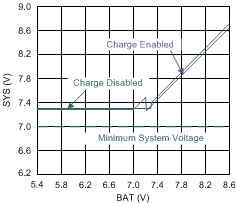
GUID-D0457B2E-442C-4564-8005-E7B40ADF6B21-low.gif Figure 9-6 Typical System Voltage vs Battery Voltage for a 2S Battery Configuration