SLUSDH9D September 2019 – November 2023 UCC21750-Q1
PRODUCTION DATA
- 1
- 1 Features
- 2 Applications
- 3 Description
- 4 Revision History
- 5 Pin Configuration and Functions
-
6 Specifications
- 6.1 Absolute Maximum Ratings
- 6.2 ESD Ratings
- 6.3 Recommended Operating Conditions
- 6.4 Thermal Information
- 6.5 Power Ratings
- 6.6 Insulation Specifications
- 6.7 Safety Limiting Values
- 6.8 Electrical Characteristics
- 6.9 Safety-Related Certifications
- 6.10 Switching Characteristics
- 6.11 Insulation Characteristics Curves
- 6.12 Typical Characteristics
- 7 Parameter Measurement Information
-
8 Detailed Description
- 8.1 Overview
- 8.2 Functional Block Diagram
- 8.3
Feature Description
- 8.3.1 Power Supply
- 8.3.2 Driver Stage
- 8.3.3 VCC and VDD Undervoltage Lockout (UVLO)
- 8.3.4 Active Pulldown
- 8.3.5 Short Circuit Clamping
- 8.3.6 Internal Active Miller Clamp
- 8.3.7 Desaturation (DESAT) Protection
- 8.3.8 Soft Turn-Off
- 8.3.9 Fault (FLT, Reset, and Enable (RST/EN)
- 8.3.10 Isolated Analog to PWM Signal Function
- 8.4 Device Functional Modes
-
9 Applications and Implementation
- 9.1 Application Information
- 9.2
Typical Application
- 9.2.1 Design Requirements
- 9.2.2
Detailed Design Procedure
- 9.2.2.1 Input Filters for IN+, IN–, and RST/EN
- 9.2.2.2 PWM Interlock of IN+ and IN–
- 9.2.2.3 FLT, RDY, and RST/EN Pin Circuitry
- 9.2.2.4 RST/EN Pin Control
- 9.2.2.5 Turn-On and Turn-Off Gate Resistors
- 9.2.2.6 Overcurrent and Short Circuit Protection
- 9.2.2.7 Isolated Analog Signal Sensing
- 9.2.2.8 Higher Output Current Using an External Current Buffer
- 9.2.3 Application Curves
- 10Power Supply Recommendations
- 11Layout
- 12Device and Documentation Support
- 13Mechanical, Packaging, and Orderable Information
9.2.2.2 PWM Interlock of IN+ and IN–
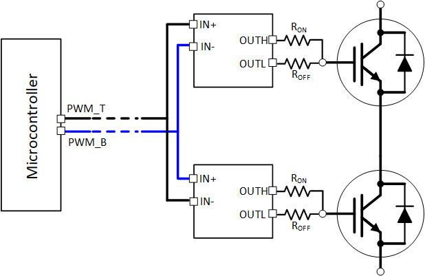
The UCC21750-Q1 features the PWM interlock for IN+ and IN– pins, which can be used to prevent the phase leg shoot through issue. As shown in Table 8-1, the output is logic low while both IN+ and IN– are logic high. When only IN+ is used, IN– can be tied to GND. To use the PWM interlock function, the PWM signal of the other switch in the phase leg can be sent to the IN– pin. As shown in Figure 9-2, the PWM_T is the PWM signal to top side switch, the PWM_B is the PWM signal to bottom side switch. For the top side gate driver, the PWM_T signal is given to the IN+ pin, while the PWM_B signal is given to the IN- pin; for the bottom side gate driver, the PWM_B signal is given to the IN+ pin, while PWM_T signal is given to the IN- pin. When both PWM_T and PWM_B signals are high, the outputs of both gate drivers are logic low to prevent the shoot through condition.
 Figure 9-2 PWM Interlock for a Half Bridge