SLUSE26C June   2021  – January 2022 UCC27614

PRODUCTION DATA  

  1. Features
  2. Applications
  3. Description
  4. Revision History
  5. Pin Configuration and Functions
  6. Specifications
    1. 6.1 Absolute Maximum Ratings
    2. 6.2 ESD Ratings
    3. 6.3 Recommended Operating Conditions
    4. 6.4 Thermal Information
    5. 6.5 Electrical Characteristics
    6. 6.6 Switching Characteristics
    7. 6.7 Timing Diagrams
    8. 6.8 Typical Characteristics
  7. Detailed Description
    1. 7.1 Overview
    2. 7.2 Functional Block Diagram
    3. 7.3 Feature Description
      1. 7.3.1 VDD Undervoltage Lockout
      2. 7.3.2 Input Stage
      3. 7.3.3 Enable Function
      4. 7.3.4 Output Stage
    4. 7.4 Device Functional Modes
  8. Applications and Implementation
    1. 8.1 Application Information
    2. 8.2 Typical Application
      1. 8.2.1 Driving MOSFET/IGBT/SiC MOSFET
        1. 8.2.1.1 Design Requirements
        2. 8.2.1.2 Detailed Design Procedure
          1. 8.2.1.2.1 Input-to-Output Configuration
          2. 8.2.1.2.2 Input Threshold Type
          3. 8.2.1.2.3 VDD Bias Supply Voltage
          4. 8.2.1.2.4 Peak Source and Sink Currents
          5. 8.2.1.2.5 Enable and Disable Function
          6. 8.2.1.2.6 Propagation Delay and Minimum Input Pulse Width
          7. 8.2.1.2.7 Power Dissipation
        3. 8.2.1.3 Application Curves
  9. Power Supply Recommendations
  10. 10Layout
    1. 10.1 Layout Guidelines
    2. 10.2 Layout Example
    3. 10.3 Thermal Consideration
  11. 11Device and Documentation Support
    1. 11.1 Third-Party Products Disclaimer
    2. 11.2 Receiving Notification of Documentation Updates
    3. 11.3 Support Resources
    4. 11.4 Trademarks
    5. 11.5 Electrostatic Discharge Caution
    6. 11.6 Glossary
  12. 12Mechanical, Packaging, and Orderable Information

Typical Characteristics

Unless otherwise specified, VDD = 12 V, IN+ = 3.3 V, IN- = GND, TJ = 25 °C, No load

GUID-82072325-8ABC-4387-8F9A-8C4969F16F89-low.gifFigure 6-4 Peak Source Current vs VDD
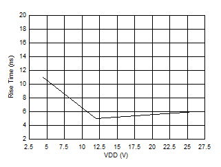
GUID-8E3A52B8-0345-4F74-9D08-55E006C8E449-low.gif
CLOAD = 1.8 nF
Figure 6-6 Output Rise Time vs VDD
GUID-20211110-SS0I-MWGS-WNBS-FXSTKLCPN07N-low.png
CLOAD = 1.8 nF
Figure 6-8 Output Rise and Fall Time vs Temperature
GUID-FDF53194-5036-4E84-9574-ADDDC2F1DF3A-low.gif
CLOAD = 1.8 nF
Figure 6-10 Falling (Turnoff) Propagation Delay vs VDD
GUID-69F6446F-635F-4F0E-8228-83021306B26E-low.gifFigure 6-12 Operating Supply Current vs VDD
GUID-6081944B-9E82-46A7-983F-4AB018A5FFE8-low.gifFigure 6-14 Input Threshold vs VDD
GUID-20210526-CA0I-XLDP-WXVW-RM9TS7GGRDBN-low.pngFigure 6-16 Input Threshold Hysteresis vs Temperature
GUID-20210526-CA0I-1F64-GC7R-KGGMXZRGDPXJ-low.pngFigure 6-18 Output Pullup Resistance vs Temperature
GUID-20210526-CA0I-3VTD-CMZM-BTJFKGNCX6DV-low.pngFigure 6-20 Output Pulldown Resistance vs Temperature
GUID-20210526-CA0I-XMWP-ZXGS-SJCCWTXPGJQM-low.pngFigure 6-22 UVLO Hysteresis vs Temperature
GUID-8072D77A-21C3-4953-AA5B-87706E4D4FA3-low.gifFigure 6-5 Peak Sink Current vs VDD
GUID-81C2C69D-42CA-4DE6-9654-A1E48DA9BAD7-low.gif
CLOAD = 1.8 nF
Figure 6-7 Output Fall Time vs VDD
GUID-79ACAB0D-8C06-4D72-AEED-E25E525AA49F-low.gif
CLOAD = 1.8 nF
Figure 6-9 Rising (Turnon) Propagation Delay vs VDD
GUID-20210526-CA0I-6GQC-6SFT-HBP5NH5QPN6D-low.png
CLOAD = 1.8 nF
Figure 6-11 Propagation Delay vs Temperature
GUID-20211110-SS0I-QQK7-NBLT-82RW0SSLRZZL-low.pngFigure 6-13 Operating Static Supply Current vs Temperature
GUID-20210526-CA0I-0TKQ-KPVC-NTMHN1WMDL5X-low.pngFigure 6-15 Input Threshold vs Temperature
GUID-C84C2C46-E65A-4F6C-A6AC-002E4A1920D4-low.gifFigure 6-17 Output Pullup Resistance vs VDD
GUID-20211110-SS0I-6M34-GQZM-HNMZHHJ564C8-low.pngFigure 6-19 Output Pulldown Resistance vs VDD
GUID-20210526-CA0I-ZDLX-JVTK-PHCSL4V3NLZR-low.pngFigure 6-21 UVLO Threshold vs Temperature