SLUSES3B October 2023 – July 2024 UCC25660
PRODUCTION DATA
- 1
- 1 Features
- 2 Applications
- 3 Description
- 4 Device Comparison Table
- 5 Pin Configuration and Functions
- 6 Specifications
-
7 Detailed Description
- 7.1 Overview
- 7.2 Functional Block Diagram
- 7.3 Feature Description
- 7.4 Protections
- 7.5 Device Functional Modes
-
8 Application and Implementation
- 8.1 Application Information
- 8.2
Typical Application
- 8.2.1 Design Requirements
- 8.2.2
Detailed Design Procedure
- 8.2.2.1 LLC Power Stage Requirements
- 8.2.2.2 LLC Gain Range
- 8.2.2.3 Select Ln and Qe
- 8.2.2.4 Determine Equivalent Load Resistance
- 8.2.2.5 Determine Component Parameters for LLC Resonant Circuit
- 8.2.2.6 LLC Primary-Side Currents
- 8.2.2.7 LLC Secondary-Side Currents
- 8.2.2.8 LLC Transformer
- 8.2.2.9 LLC Resonant Inductor
- 8.2.2.10 LLC Resonant Capacitor
- 8.2.2.11 LLC Primary-Side MOSFETs
- 8.2.2.12 Design Considerations for Adaptive Dead-Time
- 8.2.2.13 LLC Rectifier Diodes
- 8.2.2.14 LLC Output Capacitors
- 8.2.2.15 HV Pin Series Resistors
- 8.2.2.16 BLK Pin Voltage Divider
- 8.2.2.17 ISNS Pin Differentiator
- 8.2.2.18 TSET Pin
- 8.2.2.19 OVP/OTP Pin
- 8.2.2.20 Burst Mode Programming
- 8.2.2.21 Application Curves
- 8.3 Power Supply Recommendations
- 8.4 Layout
- 9 Revision History
- 10Mechanical, Packaging, and Orderable Information
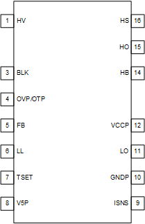
5 Pin Configuration and Functions
 Figure 5-1 DDB Package16-Pin SOIC (Pins 2, 13
removed)Top
View
Figure 5-1 DDB Package16-Pin SOIC (Pins 2, 13
removed)Top
View| PIN | I/O | DESCRIPTION | |
|---|---|---|---|
| NAME | NO. | ||
| HV | 1 | I |
High-voltage (HV) Startup and X-Capacitor Discharge. This pin is used to to perform HV startup. After startup is completed, the HV pin is used for AC presence detection and X-Capacitor discharge. This pin is connected to the rectified AC line ( for UCC256601 and 604) or input bulk capacitor ( for UCC256602). |
| 2 | - | Missing. HV spacer for creepage between high voltage and low voltage pins | |
| BLK | 3 | I |
Bulk input UVLO/OVLO and input voltage feedforward. This pin is connected to a resistor divider that looks at bulk capacitor voltage. |
| OVP/OTP | 4 | I |
Overvoltage protection and external overtemperature protection. This pin connects through an NTC resistor to ground and to a Zener diode that connects to VCC |
| FB | 5 | I |
Feedback signal. This pin is connected to the collector of an opto-coupler. This pin is for feedback input. |
| LL | 6 | I |
Light load operation options and burst mode threshold setting. This pin is connected to an external resistor divider. The top resistor of the divider is connected to V5P. The impedance and voltage of this pin is used to select the theresholds for high frequncy and low frequency burst mode operation . |
| TSET | 7 | I/O |
This pin is used to program the internal resonant tank current integrator (VCR synthesizer) time constant and minimum switching frequency. Depending on the option programmed, the maximum deadtime is also selected. After the programming phase ends, TSET pin provides PFC on/off signal in the UCC256604 variant. |
| V5P | 8 | P |
5V bias. This pin is externally connected to a decoupling capacitor to GNDP. |
| ISNS | 9 | I |
Resonant current sensing. This pin senses the differentiated resonant capacitor voltage.This signal is internally used to: 1. Generate the control signal. 2. OCP & Cycle-by-Cycle current limiting. 3. Capacitive region avoidance. |
| GNDP | 10 | P | This pin is connected to primary-side bulk capacitor negative terminal |
| LO | 11 | O | Low-side gate driver output. |
| VCCP | 12 | P |
IC supply voltage This pin is connected to a decoupling capacitor. For applications including a bias winding on the LLC transformer, the VCC pin is connected through a diode to the bias winding. For applications where HV startup is disabled, VCCP is supplied by an auxilliary bias supply. The VCCP pin is internally clamped to 19V. |
| 13 | N/A | Missing pin. High-voltage spacer for creepage between high-voltage and low-voltage pins. | |
| HB | 14 | P | High-side gate driver bias. A capacitor connecting between HB and HS provides the high-side driver energy. |
| HO | 15 | O | High-side gate driver output. |
| HS | 16 | P |
High-side gate driver return. This pin is connected to the switch node of the half-bridge structure in the LLC power stage. |
Please refere to section 8.2 Typical Application for more details.