SLUSFS6 October   2024 TPS62A04AB , TPS62A04B

PRODUCTION DATA  

  1.   1
  2. Features
  3. Applications
  4. Description
  5. Device Comparison Table
  6. Pin Configuration and Functions
  7. Specifications
    1. 6.1 Absolute Maximum Ratings
    2. 6.2 ESD Ratings
    3. 6.3 Recommended Operating Conditions
    4. 6.4 Thermal Information
    5. 6.5 Electrical Characteristics
    6. 6.6 Typical Characteristics
  8. Detailed Description
    1. 7.1 Overview
    2. 7.2 Functional Block Diagram
    3. 7.3 Feature Description
      1. 7.3.1 Power Save Mode
      2. 7.3.2 100% Duty Cycle Low Dropout Operation
      3. 7.3.3 Soft Start
      4. 7.3.4 Switch Current Limit and Short-Circuit Protection (HICCUP)
      5. 7.3.5 Undervoltage Lockout
      6. 7.3.6 Thermal Shutdown
    4. 7.4 Device Functional Modes
      1. 7.4.1 Enable and Disable
      2. 7.4.2 Power Good
  9. Application and Implementation
    1. 8.1 Application Information
    2. 8.2 Typical Application
      1. 8.2.1 Design Requirements
      2. 8.2.2 Detailed Design Procedure
        1. 8.2.2.1 Setting the Output Voltage
        2. 8.2.2.2 Feedforward Capacitor
        3. 8.2.2.3 Output Filter Design
        4. 8.2.2.4 Input and Output Capacitor Selection
      3. 8.2.3 Application Curves
    3. 8.3 Power Supply Recommendations
    4. 8.4 Layout
      1. 8.4.1 Layout Guidelines
      2. 8.4.2 Layout Example
  10. Device and Documentation Support
    1. 9.1 Device Support
      1. 9.1.1 Third-Party Products Disclaimer
    2. 9.2 Documentation Support
      1. 9.2.1 Related Documentation
    3. 9.3 Receiving Notification of Documentation Updates
    4. 9.4 Support Resources
    5. 9.5 Trademarks
    6. 9.6 Electrostatic Discharge Caution
    7. 9.7 Glossary
  11. 10Revision History
  12. 11Mechanical, Packaging, and Orderable Information

Application Curves

VIN = 5.0V, VOUT = 1.2V, TA = 25°C, BOM = Table 8-2 unless otherwise noted.

TPS62A04B TPS62A04AB 0.6V Output Efficiency (TPS62A04B) Figure 8-2 0.6V Output Efficiency (TPS62A04B)
TPS62A04B TPS62A04AB 1.8V Output Efficiency (TPS62A04B) Figure 8-4 1.8V Output Efficiency (TPS62A04B)
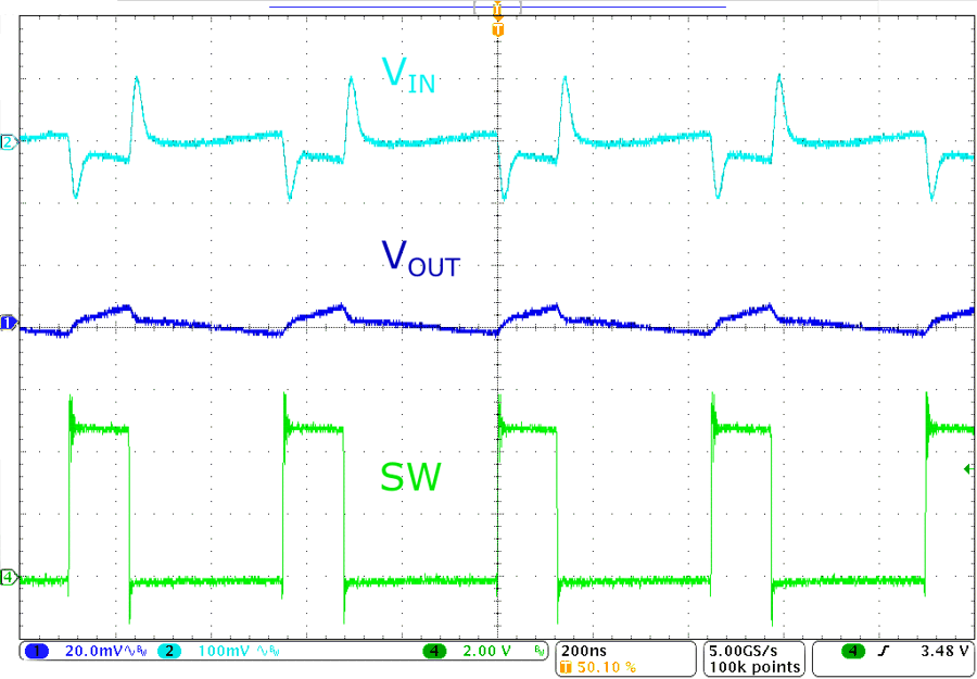
TPS62A04B TPS62A04AB PWM Operation (TPS62A04B)
Load Current = 4A
Figure 8-6 PWM Operation (TPS62A04B)
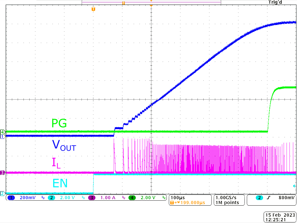
TPS62A04B TPS62A04AB Start-Up With No Load (TPS62A04B)Figure 8-8 Start-Up With No Load (TPS62A04B)
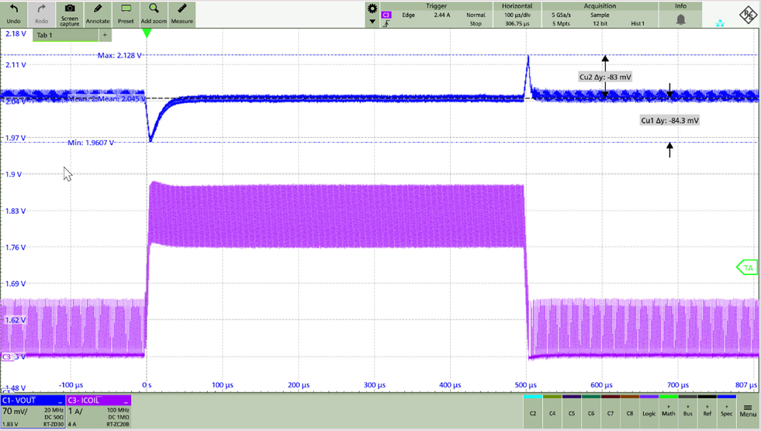
TPS62A04B TPS62A04AB Load Transient
                                    Response (TPS62A04B)
Load Step: 0.3A to 3.5A, 0.5A/µs
L = TFM160808BLE-R24 (240nH, 1608), COUT = 4 ×10μF
Figure 8-10 Load Transient Response (TPS62A04B)
TPS62A04B TPS62A04AB Safe Operating Area Based on EVM,
                                                  VIN = 3.3V, TPS62A04xBDRL
RθJA = 74.5°C/WTJmax = 125°C
Figure 8-12 Safe Operating Area Based on EVM, VIN = 3.3V, TPS62A04xBDRL
TPS62A04B TPS62A04AB 1.2V Output Efficiency (TPS62A04B) Figure 8-3 1.2V Output Efficiency (TPS62A04B)
TPS62A04B TPS62A04AB 1.8V Output Efficiency (TPS62A04AB) Figure 8-5 1.8V Output Efficiency (TPS62A04AB)
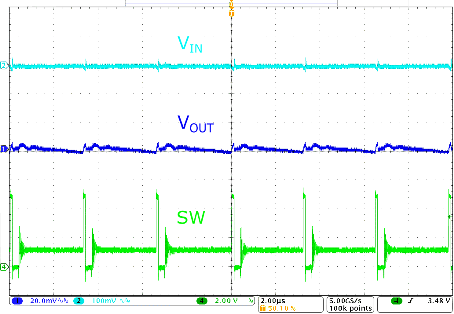
TPS62A04B TPS62A04AB PFM Operation (TPS62A04B)
Load Current = 100mA
Figure 8-7 PFM Operation (TPS62A04B)
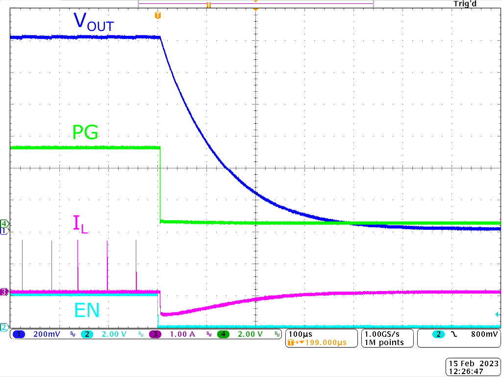
TPS62A04B TPS62A04AB Shutdown With No Load (TPS62A04B)Figure 8-9 Shutdown With No Load (TPS62A04B)
TPS62A04B TPS62A04AB Safe Operating Area Based on EVM,
                                                  VIN = 5.0V, TPS62A04xBDRL
RθJA = 74.5°C/WTJmax = 125°C
Figure 8-11 Safe Operating Area Based on EVM, VIN = 5.0V, TPS62A04xBDRL