SLUUC77 July 2020 – MONTH LMR50410-Q1
4 Board Layout
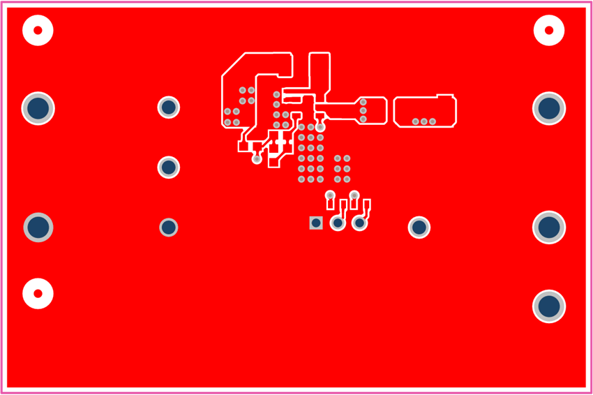
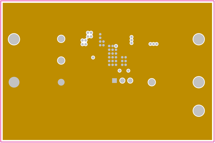
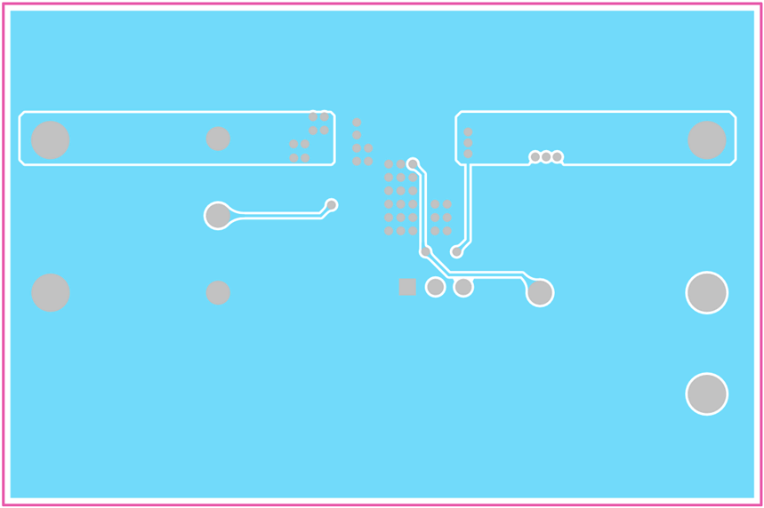
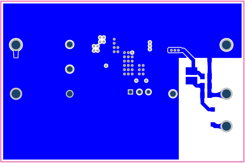
Figure 4-1to Figure 4-4 show the board layout for the LMR50410QEVM. The PCB consists of a 4-layer design. The board size is 46-mm x 69-mm, 2-oz copper planes are applied on top and bottom layers, 1-oz copper planes are applied on middle layers.
 Figure 4-1 Top Layer
 Figure 4-2 Middle Layer One
 Figure 4-3 Middle Layer Two
 Figure 4-4 Bottom Layer