SLUUCP7A August 2023 – March 2024 LMR51606
4 Board Layout
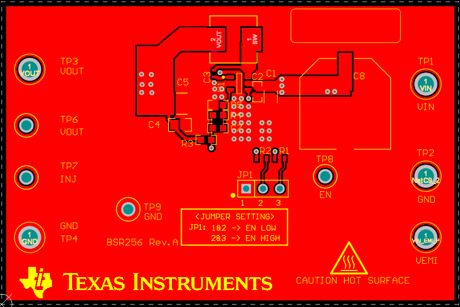
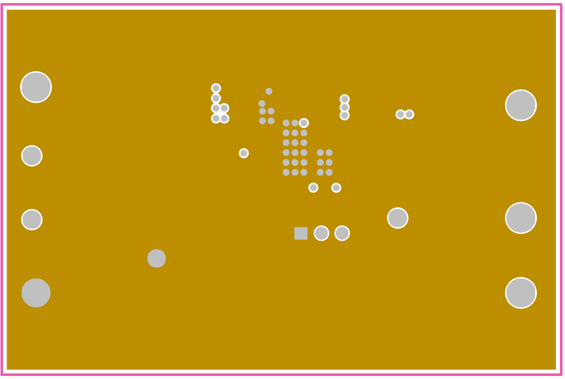
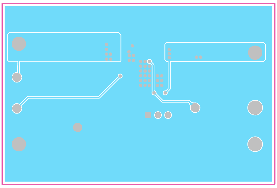
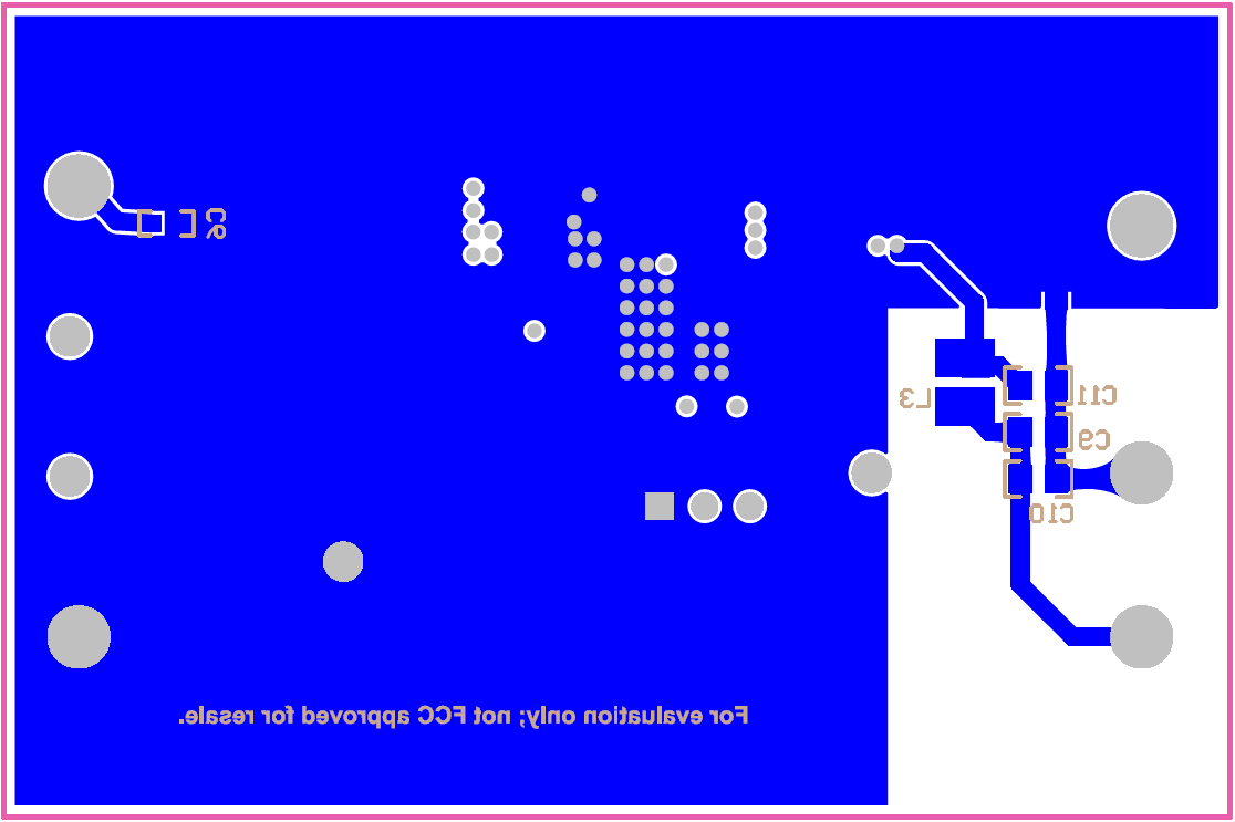
Figure 4-1andFigure 4-4 show the board layout for the LMR51606YEVM. The PCB consists of a 4-layer design. The board size is 46 mm × 69 mm. 2-oz copper planes are applied on top and bottom layers, 1-oz copper planes are applied on middle layers.
 Figure 4-1 Top
Layer
 Figure 4-2 Middle Layer One
 Figure 4-3 Middle Layer Two
 Figure 4-4 Bottom Layer