SLUUCT6 April 2024 BQ25186
4.2 PCB Layout
Figure 5-4 through Figure 5-9 show the EVM PCB layout images.
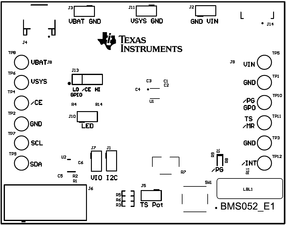 Figure 4-4 Top Overlay
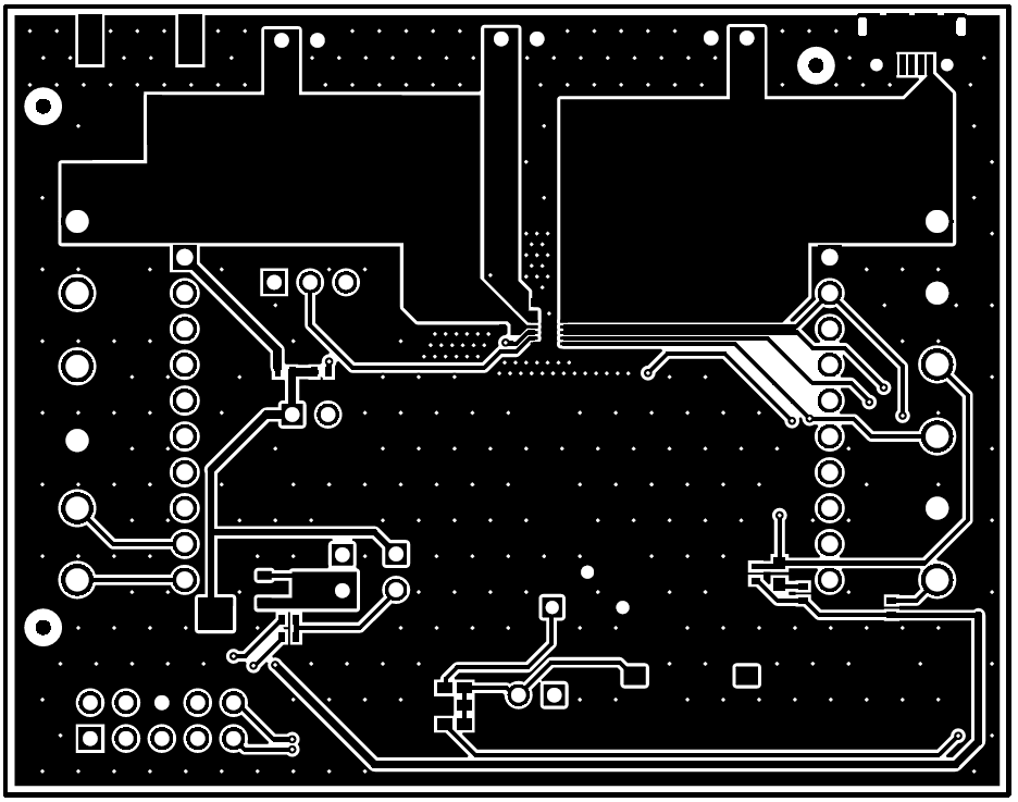 Figure 4-6 Top Layer
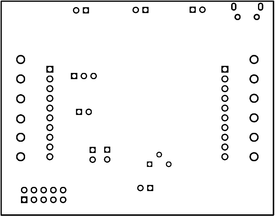 Figure 4-8 Bottom Solder
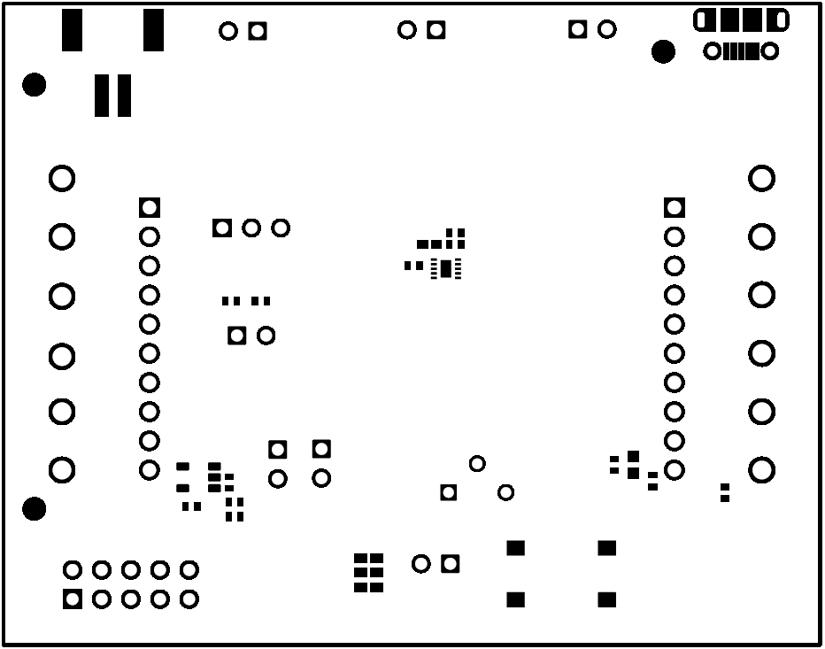 Figure 4-5 Top Solder
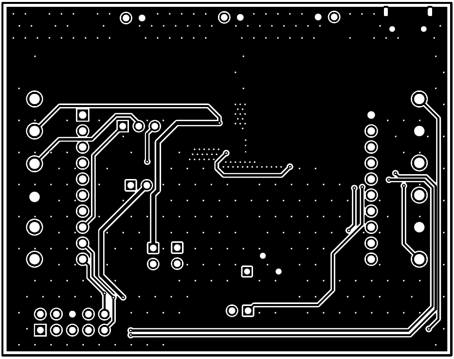 Figure 4-7 Bottom Layer
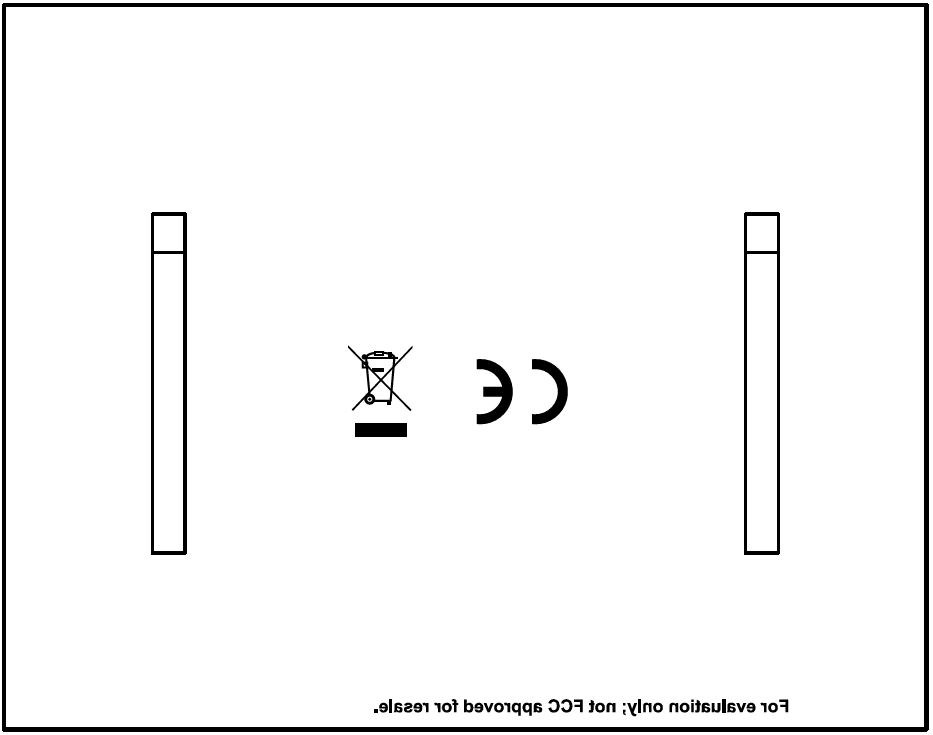 Figure 4-9 Bottom Overlay
SLUUCT6 April 2024 BQ25186
Figure 5-4 through Figure 5-9 show the EVM PCB layout images.
 Figure 4-4 Top Overlay
 Figure 4-6 Top Layer
 Figure 4-8 Bottom Solder
 Figure 4-5 Top Solder
 Figure 4-7 Bottom Layer
 Figure 4-9 Bottom Overlay