SLUUD40 July   2024 TPSM82813 , TPSM82816


  1.   1
  2.   Description
  3.   Features
  4.   4
  5. 1Evaluation Module Overview
    1. 1.1 Introduction
    2. 1.2 Kit Contents
    3. 1.3 Specification
    4. 1.4 Device Information
  6. 2Hardware
    1. 2.1 Safety Instructions
    2. 2.2 Header Information
    3. 2.3 Jumper Information
    4. 2.4 Test Points
  7. 3Implementation Results
    1. 3.1 Performance Data and Results
    2. 3.2 Modifications
      1. 3.2.1 Input and Output Capacitors
      2. 3.2.2 Switching Frequency, Spread Spectrum and Control Loop Compensation
      3. 3.2.3 Soft-Start Time
      4. 3.2.4 Loop Response Measurement
      5. 3.2.5 Precise Turn-on Voltage
  8. 4Hardware Design Files
    1. 4.1 Schematic
    2. 4.2 Board Layout
    3. 4.3 Bill of Materials
  9. 5Additional Information
    1. 5.1 Trademarks

Board Layout

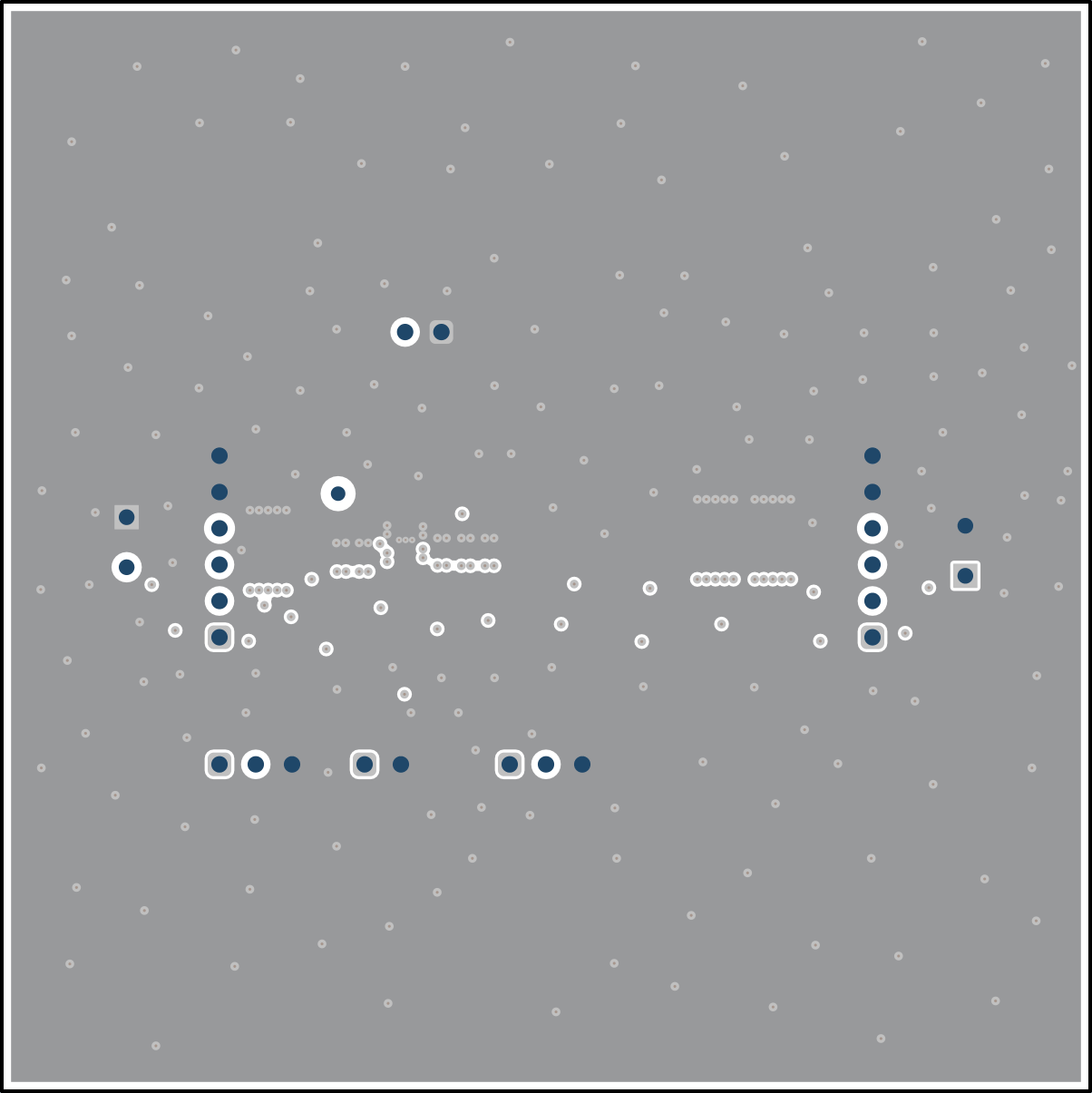
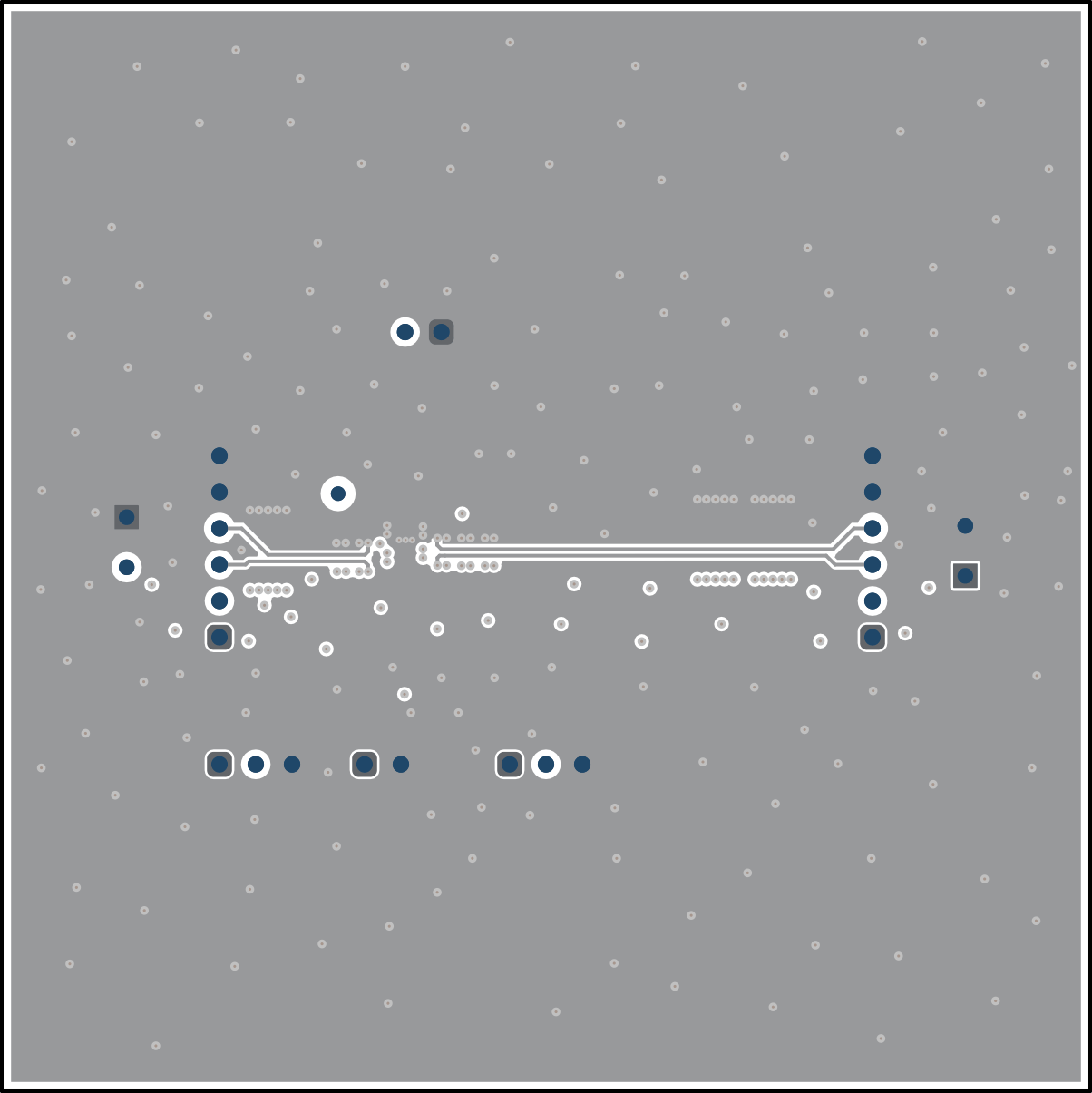
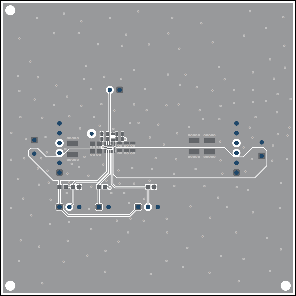
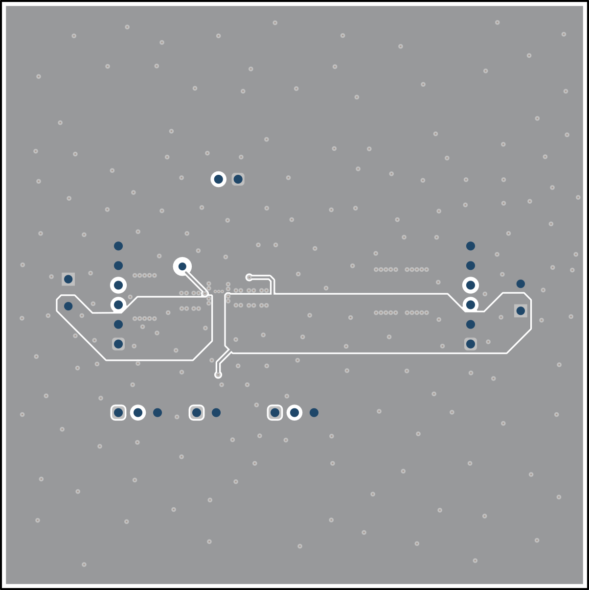
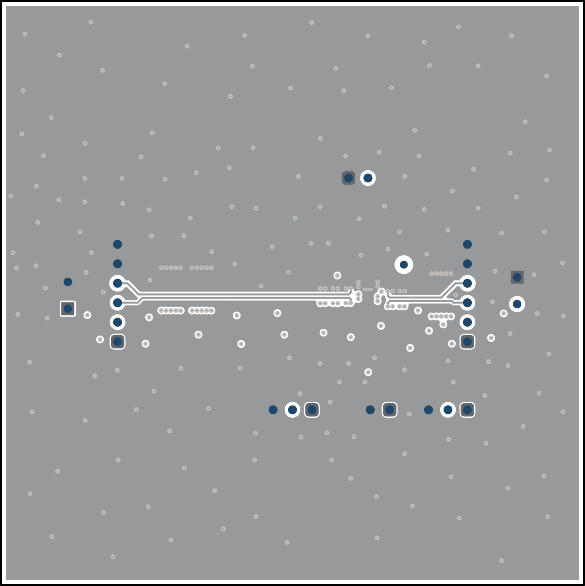
This section provides the TPSM8281xPEVM-062 board layout. The Gerber files are available on the TPSM82816PEVM-062 tool folder. All four layers use 2-ounce copper.
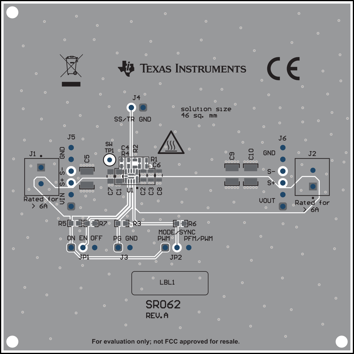
TPSM82813PEVM-062, TPSM82816PEVM-062 Top AssemblyFigure 4-2 Top Assembly
TPSM82813PEVM-062, TPSM82816PEVM-062 Internal Layer 1Figure 4-4 Internal Layer 1
TPSM82813PEVM-062, TPSM82816PEVM-062 Bottom LayerFigure 4-6 Bottom Layer
TPSM82813PEVM-062, TPSM82816PEVM-062 Top LayerFigure 4-3 Top Layer
TPSM82813PEVM-062, TPSM82816PEVM-062 Internal Layer 2Figure 4-5 Internal Layer 2
TPSM82813PEVM-062, TPSM82816PEVM-062 Bottom Layer (Mirrored)Figure 4-7 Bottom Layer (Mirrored)