SLVA478C October 2013 – November 2022 TPS62120 , TPS62122
5 Typical Performance and Waveforms
The application circuit shown in Figure 5-1 is used to generate the data presented in Figure 5-2 – Figure 5-7. The output capacitor used is a 10-µF, 6.3-V, 0603, X5R ceramic capacitor. For a 5-V output, loss of capacitance from the DC bias effect can be significant. Unless otherwise specified, VIN = 5 V and VOUT = –5 V.
 Figure 5-1 Schematic of the Tested Circuit
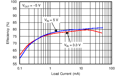 Figure 5-2 Efficiency versus Load Current with VOUT = –5 V
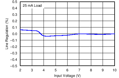 Figure 5-3 Line Regulation with VOUT = –5 V and 25-mA Load
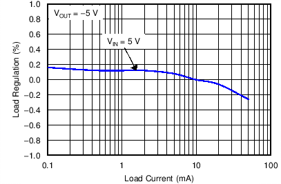 Figure 5-4 Load Regulation with VOUT = –5 V
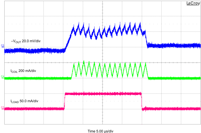 Figure 5-5 Load Transient Response 0 mA to 50 mA with VIN = 5 V
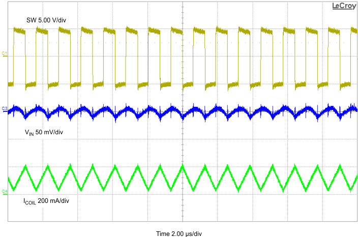 Figure 5-6 Input Voltage Ripple, VIN = 5 V and IOUT = 50 mA
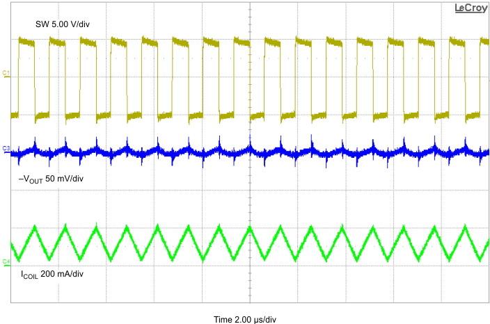 Figure 5-7 Output Voltage Ripple, VIN = 5 V and IOUT = 50 mA