SLVA478C October   2013  – November 2022 TPS62120 , TPS62122


  1.   Using the TPS62120 in an Inverting Buck-Boost Topology
  2.   Trademarks
  3. 1Inverting Buck-Boost Topology
    1. 1.1 Design Considerations
    2. 1.2 Concept
    3. 1.3 Output Current Calculations
    4. 1.4 VIN and VOUT Range
  4. 2Digital Pin Configurations
    1. 2.1 Enable Pin
    2. 2.2 SGND Pin
    3. 2.3 Power Good Pin
  5. 3Startup Behavior and Switching Node Consideration
  6. 4External Component Selection
    1. 4.1 Inductor Selection
    2. 4.2 Input Capacitor Selection
    3. 4.3 Selecting L and COUT for Stability
  7. 5Typical Performance and Waveforms
  8. 6Conclusion
  9. 7References
  10. 8Revision History

SGND Pin

SGND is an NMOS open-drain output pin that can be used to discharge the output capacitor. The internal NMOS connects the SGND pin to the IC ground (which is VOUT) once the device is shutdown. It becomes high impedance once the device is enabled. The SGND pin should be connected to ground to operate this discharge function in the same way as a buck converter. If not used, SGND may be left floating or connected to VOUT. Figure 2-4 shows the SGND internal circuit.
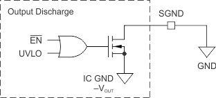
GUID-F99336B2-AB46-4248-8D38-E5355C42A463-low.gifFigure 2-4 SGND Internal Circuit