SLVAEO9B February 2020 – January 2021 TPS62065-Q1 , TPS62067-Q1
4 Pin Failure Mode Analysis (Pin FMA)
This section provides a Failure Mode Analysis (FMA) for the pins of the TPS6206x-Q1. The failure modes covered in this document include the typical pin-by-pin failure scenarios:
- Pin short-circuited to PGND or AGND (see Table 4-2)
- Pin open-circuited (see Table 4-3)
- Pin short-circuited to an adjacent pin (see Table 4-4)
- Pin short-circuited to AVIN or PVIN (see Table 4-5)
Table 4-2 through Table 4-5 also indicate how these pin conditions can affect the device as per the failure effects classification in Table 4-1.
| Class | Failure Effects |
|---|---|
| A | Potential device damage that affects functionality |
| B | No device damage, but loss of functionality |
| C | No device damage, but performance degradation |
| D | No device damage, no impact to functionality or performance |
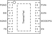
Figure 4-1 shows the TPS6206x-Q1 pin diagram. For a detailed description of the device pins please refer to the 'Pin Configuration and Functions' section in the TPS6206x-Q1 data sheet.
 Figure 4-1 Pin Diagram
Following are the assumptions of use and the device configuration assumed for the pin FMA in this section:
- Assumption the device is running in the typical application. Please refer to the 'Typical Application Circuit' on the 1st page in the TPS6206x-Q1 datasheet.
| Pin Name | Pin No. | Description of Potential Failure Effect(s) | Failure Effect Class |
|---|---|---|---|
| PGND | 1 | Intended connection | D |
| SW | 2 | Potential internal device damage | A |
| AGND | 3 | Intended connection | D |
| FB | 4 | Device not functional: Missing feedback path (Open Loop operation); output voltage out of spec; potential device damage | A |
| EN | 5 | Intended connection: Device disabled | D |
| MODE | 6 | TPS62065-Q1: Intended connection: Enabling power safe mode with automatic transition from PFM to fixed frequency PWM mode | D |
| PG | 6 | TPS62067-Q1: Intended connection in case PG not used | D |
| AVIN | 7 | Device not functional; supply short to ground | B |
| PVIN | 8 | Device not functional; supply short to ground | B |
| Pin Name | Pin No. | Description of Potential Failure Effect(s) | Failure Effect Class |
|---|---|---|---|
| PGND | 1 | Internal ground shift; device not functional; potential internal damage | A |
| SW | 2 | Device not function - open loop operation | B |
| AGND | 3 | Internal ground shift; device not functional; potential internal damage | A |
| FB | 4 | Device not functional - open loop operation | B |
| EN | 5 | Undetermined state of pin EN; spec violation; potentially increased quiescent current | C |
| MODE | 6 | TPS62065-Q1: Undetermined state of pin MODE/PG spec violation; potentially increased quiescent current | C |
| PG | 6 | TPS62067-Q1: Intended connection in case PG not used | D |
| AVIN | 7 | Missing power supply - device not functional | B |
| PVIN | 8 | Missing power supply - device not functional | B |
| Pin Name | Pin No. | Shorted to | Description of Potential Failure Effect(s) | Failure Effect Class |
|---|---|---|---|---|
| PGND | 1 | SW | Potential internal device damage | A |
| SW | 2 | AGND | Potential internal device damage | A |
| AGND | 3 | FB | Device not functional: Missing feedback path (Open Loop operation); output voltage out of spec; potential device damage | A |
| EN | 5 | MODE | TPS62065-Q1: Intended connection: Device operation in fixed frequency PWM mode | D |
| EN | 5 | PG | TPS62067-Q1: Potential internal damage | A |
| MODE | 6 | AVIN | TPS62065-Q1: Intended connection: Device operation in fixed frequency PWM mode | D |
| PG | 6 | AVIN | TPS62067-Q1: Potential internal damage | A |
| AVIN | 7 | PVIN | Intended connection | D |
| Pin Name | Pin No. | Description of Potential Failure Effect(s) | Failure Effect Class |
|---|---|---|---|
| PGND | 1 | Device not functional; supply short to ground | B |
| SW | 2 | Potential internal device damage | A |
| AGND | 3 | Device not functional; supply short to ground | B |
| FB | 4 | Device not functional: Missing feedback path (Open Loop operation); output voltage out of spec; potential device damage | A |
| EN | 5 | Intended connection: Device enabled | D |
| MODE | 6 | TPS62065-Q1: Intended connection: Device operation in fixed frequency PWM mode | D |
| PG | 6 | TPS62067-Q1: Potential internal damage | A |
| AVIN | 7 | Intended connection | D |
| PVIN | 8 | Intended connection | D |