SLVAER0B August 2020 – December 2020 TPS55288 , TPS55288-Q1 , TPS552882 , TPS552882-Q1
2.4 Power and GND Plane Design
While paying special attention to the component placement, critical traces and loop routing, inner layer GND copper plane routing is also important. Placing a whole layer GND copper plane under the switching loops establish a passive shielding for the circuit. By Lenz’s law, the current in the shield layer generates a magnetic field to counteract the original switch-loop magnetic field. The result is magnetic flux reduction and better EMI performance. Having an uninterrupted, whole GND copper plane right under the high frequency switching-loops offers the best performance.
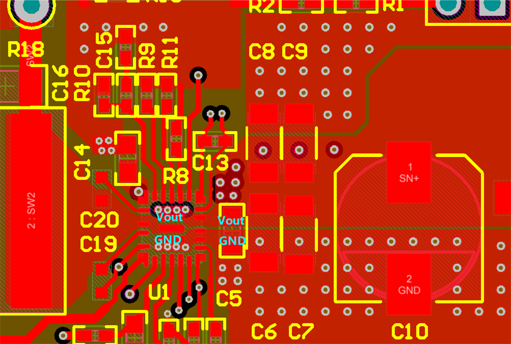
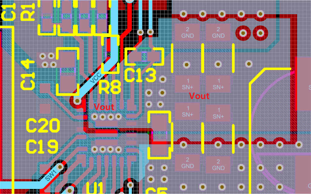
For the high-power integrated boost or buck-boost converters, thermal performance is critical to the success of the circuit design. Thermal performance determines the system reliability. TI recommends using thermal vias beneath the TPS55288 connecting PGND pin and VOUT pin to the PGND plane and a large VOUT area separately. Figure 2-7 and Figure 2-8 show examples of a proper layout with good thermal performance. Two whole GND layers are placed on layer 2 and layer 4. A large VOUT area is placed on layer 3.
 Figure 2-7 Place Thermal-Vias on the PGND
Pin
 Figure 2-8 Place Thermal-Vias on the VOUT
Pin