SLVAER0B August 2020 – December 2020 TPS55288 , TPS55288-Q1 , TPS552882 , TPS552882-Q1
2.3 Driver Circuit and Signal Circuit Routing
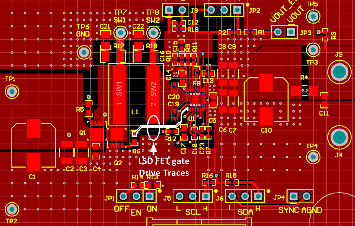
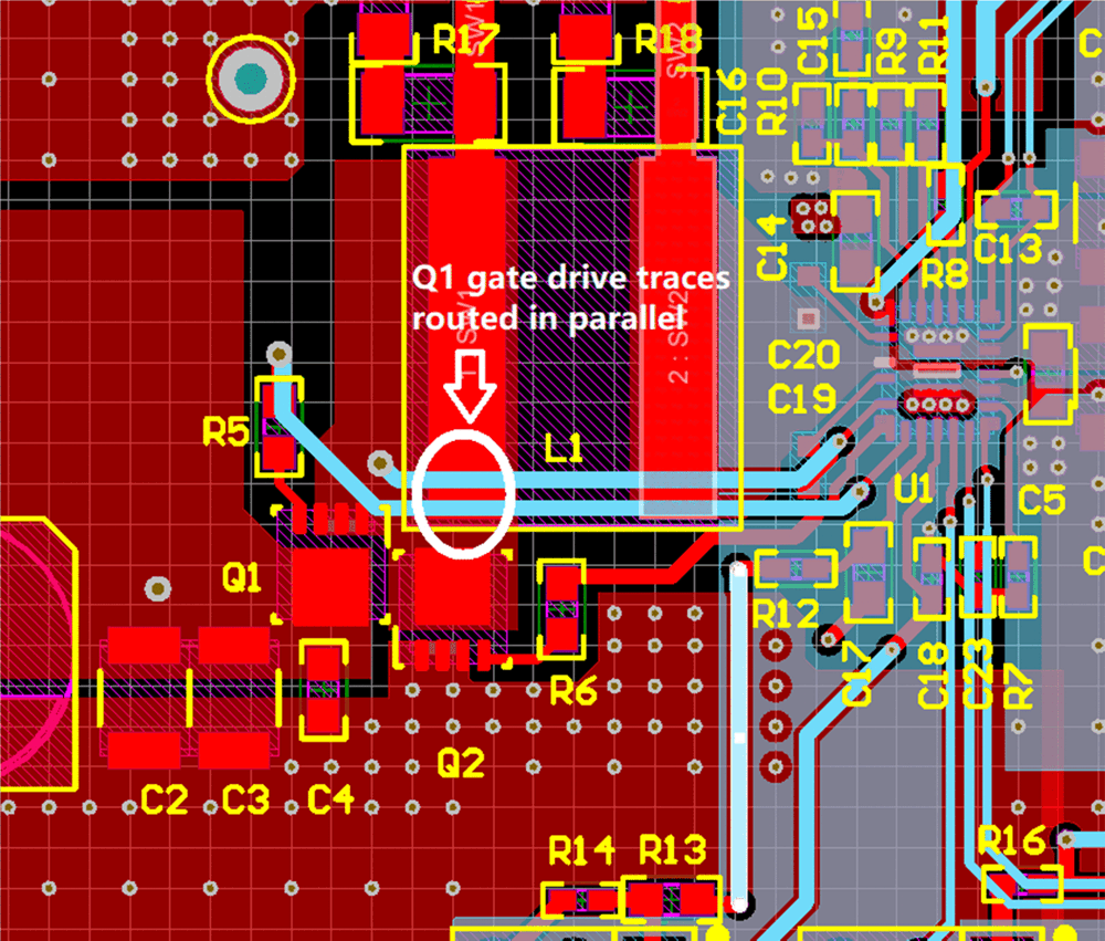
Figure 2-3 and Figure 2-4 show the gate drive traces running from the IC to the buck-leg MOSFETs. The drive traces are routed on layer 1 and 3. Kelvin – connecting the gate drive return traces directly to the respective MOSFET sources minimize common-source inductance. To minimize gate-loop area, gate and source traces are routed side by side as differential pairs. The return current for the low side MOSFET gate driver flows on the GND plane back to the PGND pin of the IC. The gate drive resistors should be placed close to the gate terminal of each MOSFET.
 Figure 2-3 Low-Side-FET Drive Traces
Routing
 Figure 2-4 High-Side-FET Drive Traces
Routing
Figure 2-4 High-Side-FET Drive Traces
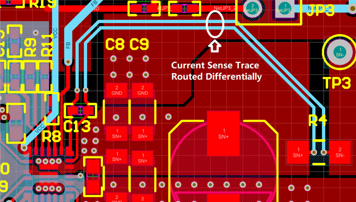
RoutingFigure 2-5 shows the traces for the output current sensing. The traces were routed as a tightly-coupled differential pair from the shut resistor to the IC, which can enhance the noise immunity and the accuracy. Place the current-sense filter capacitor close to the IC.
 Figure 2-5 Output-Current-Sense Traces
Routing
Figure 2-5 Output-Current-Sense Traces
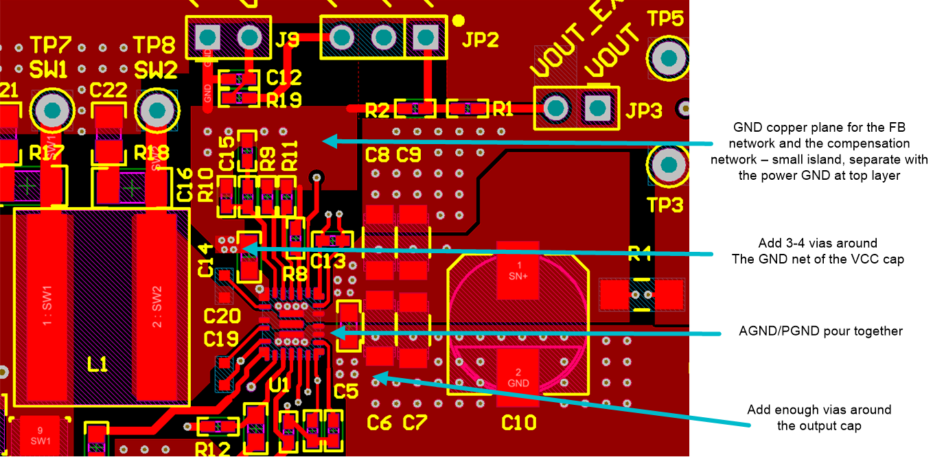
RoutingFigure 2-6 shows the AGND and the PGND connection. AGND and the PGND pin of the TPS55288 are directly poured together at the top layer. The GND net of the feedback network and the compensation network connected with the GND copper plane with vias. The VCC capacitor should be placed as close to the IC as possible. The GND net of the VCC capacitor should be directly connect with the GND plane at the inner layer through vias, so that the VCC supply current can return to the PGND of the IC with low impedance.
 Figure 2-6 AGND-PGND Connection