SLVAER4 August 2020 – MONTH TPS61022
4.2 Bench Test Results
Figure 4-3 shows the load transient waveform from 0.3 A to 0.6 A when VIN = 0.7 V. Figure 4-4 shows the load transient waveform from 0.3 A to 0.6 A when VIN = 1.5 V.
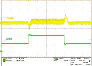 Figure 4-3 Load Transient - VIN =
0.7 V, VOUT = 3.3 V, IOUT = 0.3 A to 0.6 A
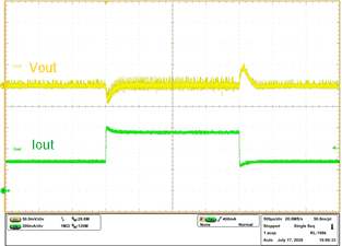 Figure 4-4 Load Transient - VIN =
1.5 V, VOUT = 3.3 V, IOUT = 0.3 A to 0.6 A
Figure 4-4 Load Transient - VIN =
1.5 V, VOUT = 3.3 V, IOUT = 0.3 A to 0.6 AFigure 4-5 shows the bode plot when VIN = 0.7 V, IOUT = 0.6 A. Figure 4-6 shows the bode plot when VIN = 0.7 V, IOUT = 0.6 A.
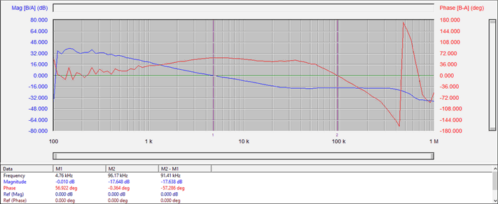 Figure 4-5 Bode Plot - VIN = 0.7
V, VOUT = 3.3V, IOUT = 0.6 A
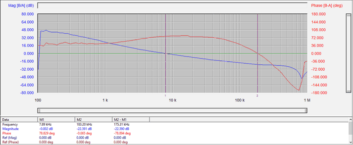 Figure 4-6 Bode Plot - VIN = 1.5
V, VOUT = 3.3 V, IOUT = 0.6 A
Figure 4-6 Bode Plot - VIN = 1.5
V, VOUT = 3.3 V, IOUT = 0.6 AFigure 4-7 shows the efficiency curve with different input voltage in auto PFM mode when VOUT = 3.3 V.
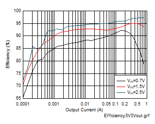 Figure 4-7 Load Efficiency With Different
Input in Auto PFM