SLVAEX2 September 2020 – MONTH TPS55288 , TPS55288-Q1 , TPS552882 , TPS552882-Q1
2.1 Radiation Theory
Some of the energy is radiated directly from the PCB, which can be modeled as a small antenna carrying the interference current. A small loop is one whose dimensions are smaller than a quarter wavelength at the frequency of interest (75cm at 100MHz). Most PCB loops count as small at emission frequencies up to a few MHz. The maximum electric field strength from such a small loop over a ground is proportional to the square of the frequency, the loop area and the current:
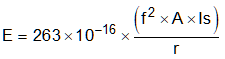
Where frequency is in Hz, A is the loop area in m2, I is in Amps and r is in meters. For square waveforms with many harmonics, the Fourier spectrum must be used for Is.
We can use Equation 1 to indicate roughly whether a PCB design is need to be improved. For example if A=4cm2, Is=10mA, f=100MHz, r=3m, therefore:

The limit line for the CISPR 22 Class B at 3 meters, is around 40 dBuV/m, 50.9 dBuV/m is over the limit. So we need do some improvement on the circuit to make the filed fall under the limit. From Equation 1, we know that the items we can control are loop area A and the high frequency current. The loop area A can be reduced by good components placement and ground shielding; the high frequency current can be reduced by slowing down the switching speed or using symmetrical switching loop placement.
Figure 2-1 (A) shows a simplified trapezoidal current waveform with period T, pulse width tW, rise time tR and fall time tF. Figure 2-1 (B) shows the frequency domain which consists of fundamental frequency and many upper harmonics. The relation with the pulse period, pulse width, rise/fall timesm and the amplitude of the upper harmonics can be derived through Fourier analysis.
Figure 2-1 is based on a 500 kHz switching signal with 1 us pulse width, 5 ns rise time and 8 ns fall time. At tRǂ tF condition, only the smaller one is considered. So the band width fR is determined by tR. Radiated EMI problems often occur in the 50 MHz~500 MHz range. It can be seen that increasing rise (or fall) time will shift the fR point to a lower frequency. Thus the high frequency harmonic content will roll-off more quickly with 40dB/dec.
 Figure 2-1 Harmonic Content of a Pulsed
Current Waveform
Figure 2-1 Harmonic Content of a Pulsed
Current Waveform