SLVAEX2 September 2020 – MONTH TPS55288 , TPS55288-Q1 , TPS552882 , TPS552882-Q1
2.2 Root Cause of the Broad Band EMI in a Buck-Boost Converter
 Figure 2-2 Buck-boost
Converter Schematic with Critical Loops
Figure 2-2 Buck-boost
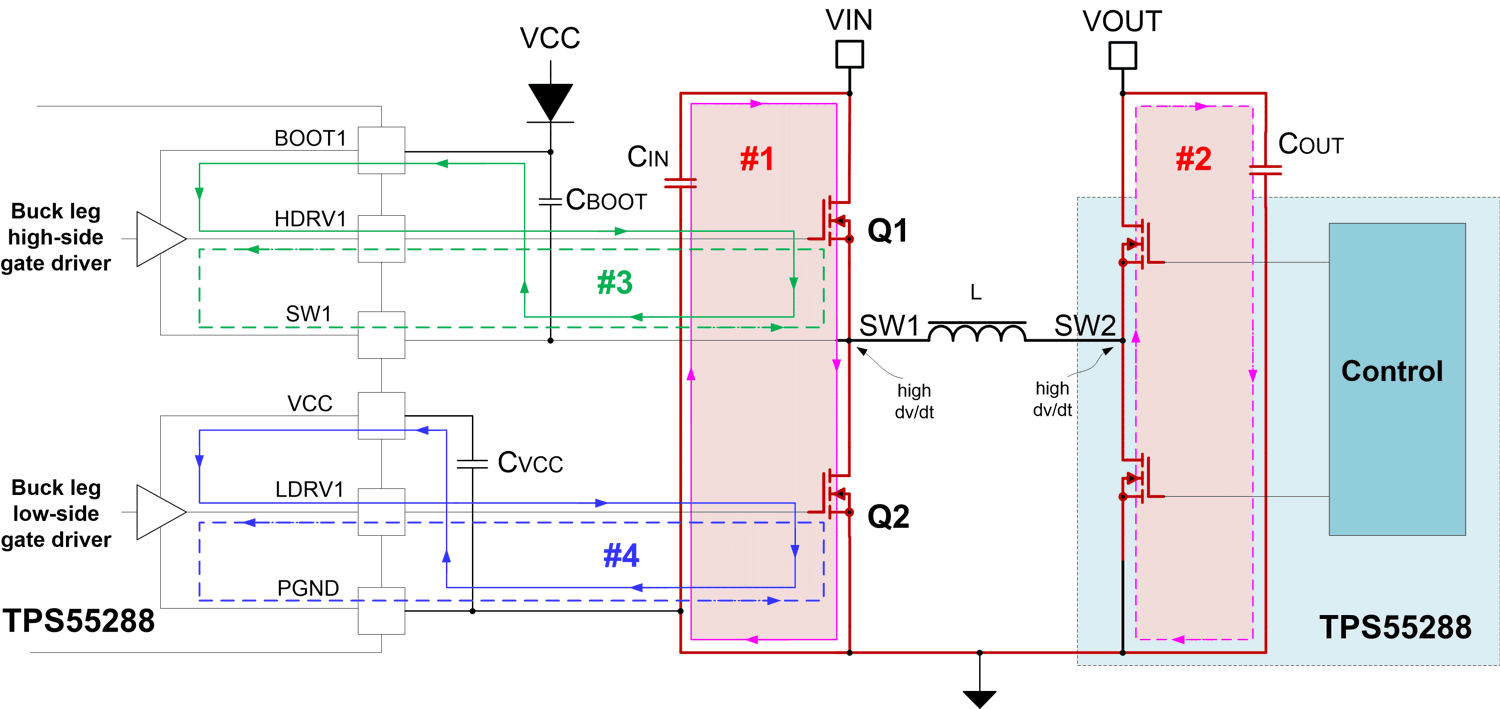
Converter Schematic with Critical LoopsFigure 2-2 shows the TPS55288 four-switch buck-boost converter with power stage components, an integrated gate drivers and a VCC bias supply. Figure 2-2 also distinguishes by color the high current traces, high dI/dt critical loops, and the high dv/dt switching nodes.
Loop 1 and loop 2, shaded in red, are the two critical high-frequency power loops for the buck-legs and the boost-legs. Long and thin traces in these two loops can cause excessive noise, overshoot and ring on the switching node, and the ground bounce because of the parasitic inductance. During a MOSFET switching event, the slew rate of the commutating current can exceed 3-5A/ns, so a 2nH parasitic inductance can results in a voltage spike of 6 V. The pulsed rectangular current waveforms flowing in these critical loops are rich in harmonic content, so a big loop area can cause big radiated energy emanating from it, which cause electromagnetic interference issue. So it is vital to minimize the trace length and the enclosed area of loop1 and loop2.
Loop 3 and 4 in Figure 2-2 are gate loops for the buck-leg MOSFET. To charge and discharge the MOSFET’s gate capacitance during turn-on and turn-off transitions, an instantaneous current up to around 1A peak flows briefly in the gate loop, which may also cause interference issue. So we also need to minimize the enclosed area of loop3 and loop4 during the trace routing.
Loop1 and loop2 are the most critical loops. Because they are in the power loop, they carry high pulsed power current. They can directly radiate, they can also interfere adjacent traces and escape into the input and output cables and cause severe EMI issue.
The maximum voltage ringing at the switching node SW1 and SW2 corresponds to the switching speed and the loop area of loop1 and loop 2. Bigger loop area will cause more severe voltage ringing at the switching node. This ringing frequency also corresponds to the frequency range which the broad band EMI centered at.