SLVAEX2 September 2020 – MONTH TPS55288 , TPS55288-Q1 , TPS552882 , TPS552882-Q1
2.3.4 Adding RC Snubbers at the Switching Node
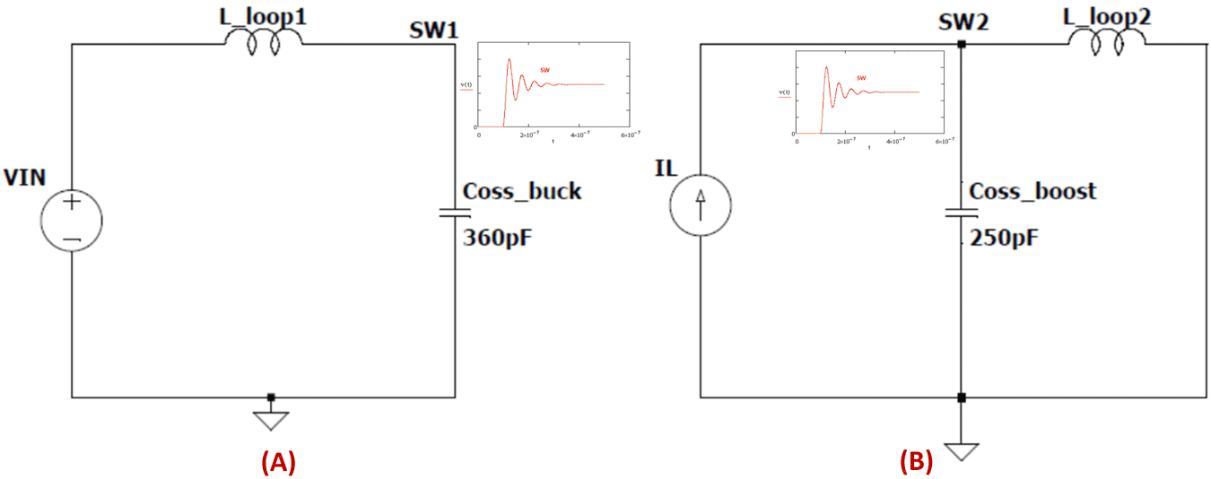
The switching loop can be modeled as an LC circuit. It is formed by the input or output side decoupling capacitor and the high-side and low-side MOSFETs. For the buck-leg switching node SW1, the ringing occurs when the high side FET is on and the low side FET is off. For the boost-leg switching node SW2, the ringing occurs when the low side FET is off and the high side FET is on. Figure 2-10 shows the equivalent model of the switching loop during this transition state.
The inductance in the equivalent model (L_loop1 and L_loop2) corresponds to the total loop inductance of the switching loop, which includes PCB trace inductance, ESL of the decoupling capacitor and package inductance of the MOSFETs. The total capacitance of the loop is determined by the output capacitance of the low side MOSFET. Therefore, the switching node ringing frequency is determined by the parasitic loop inductance and the low side MOSFET output capacitance. For a given switching speed and given MOSFET, the maximum amplitude of the ringing is also determined by the parasitic loop inductance.
From the previous chapter, we know that the we can reduce the parasitic loop inductance by compact placement, by adding ground planes under the switching loop or by using symmetrical PCB layout. But in the real application, the component placement is limited by the PCB size.
 Figure 2-10 Equivalent Model of the Switching
Loop
Figure 2-10 Equivalent Model of the Switching
LoopWhat we can do if the radiation EMI level still exceeds the requirement level and the layout cannot be improved anymore? Adding a RC snubber across the switching node and the power ground can help to reduce the radiation EMI levels. The RC snubber should be placed as close to the switching node and the ground plane as possible. Figure 2-11 shows the radiation EMI comparison result with and without RC snubber. The radiaton EMI is improved by around 6dBuV/m at 300MHz with RC snubber.
 Figure 2-11 Radiation EMI Comparison with
and without RC snubber