SLVAEX2 September 2020 – MONTH TPS55288 , TPS55288-Q1 , TPS552882 , TPS552882-Q1
2.3.1 Adding Ground Planes under the Critical Loops
We can minimize the critical loop area A by compact placement. But this method is restricted by the physical size of the components. To get low EMI, one of the most important thing we can do is adding ground planes under the switching loops. Placing whole layer GND copper planes under the switching loops establish a passive shielding for the circuit. By Lenz’s law, the current in the shield layer generates a magnetic field to counteract the original switch-loop magnetic field. The result is magnetic flux reduction, hence smaller equivalent loop area and better EMI performance.
In a multi-layer PCB with ground planes, the approximation inductance of a given loop can be calculated by Equation 3:
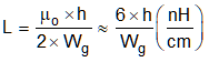
- μo=4π x 10-7
- h is the insulation thickness between the signal layer and the ground plane.
- Wg is the width of the ground plane.
From Equation 3, we can see that wider and bigger ground plane results in smaller signal loop inductance. Thinner insulation thickness between the ground plane and the signal loop also results in smaller inductance.
Table 2-1 gives out the inductance of a given loop on different PCB boards. We can see that for a 4-layer PCB with 0.4 mm insulation thickness between the signal layer and the ground plane, the trace inductance is much smaller than that of a 1.6 mm thickness 2-layer PCB. So putting a solid ground plane with minimum distance to the critical loop is one of the most effective ways to reduce the EMI.
|
PCB |
h (mm) |
Wg(mm) |
L(nH) |
|---|---|---|---|
|
2-Layer PCB |
1.6 |
10 |
4.8 |
|
4-Layer PCB |
0.4 |
10 |
1.2 |
Figure 2-3shows the cross section of a 2-layer PCB and a 4-layer PCB. Figure 2-4 shows the radiated EMI result of a 2-layer PCB, Figure 2-5 shows the radiated EMI of a 4-layer PCB. The layer-stack and the PCB cross section is similar to that of Figure 2-4. With the same component placement and same test condition, the radiated EMI is improved by more than 15dBuV/m with a 4-layer PCB.
 Figure 2-3 Cross Section of Two-Layer Board and
Four-Layer Board
Figure 2-3 Cross Section of Two-Layer Board and
Four-Layer Board Figure 2-4 Radiated EMI Result of a 2-Layer PCB
 Figure 2-5 Radiated EMI Result of a 4-Layer PCB