SLVAF13 November 2020 LM5069 , TPS1663 , TPS2663
2 Parallel Configuration
The basic principle of eFuse parallel operation and the design considerations are covered in the Achieve 20-A Circuit Protection and Space Efficiency Using Paralleled eFuses Application Report(1). The same concept is applicable for TPS26631 parallel operation. The key points from the Achieve 20-A Circuit Protection and Space Efficiency Using Paralleled eFuses Application Report(1) are summarized in the rest of this section in the context of TPS26631.
- During start-up, equal current
sharing among the parallel-connected eFuses is needed to ensure successful
start-up. To achieve that,
- The UVLO, OVP, SHDNb pins of all the parallel-connected eFuses are connected together for synchronizing the ON or OFF operation
- The dVdT pins of all the eFuses are connected together to ensure uniform output ramp rate and equal dynamic power stress
- During steady-state operation, the current sharing is decided by the RDS(on) mismatch. The device having the lower RDS(on) shares more current than the rest of the devices. However, the self-heating effect due to positive temperature characteristics of the MOSFET helps to a larger extent towards equal load current distribution in parallel configuration.
- During overload operation, the inherent current source characteristic of eFuse forces all the parallel-connected eFuses to operate in current-limiting mode. For the TPS26631, each device should have its own current-limiting resistor (RILIM) as demanded by the internal current loop architecture.
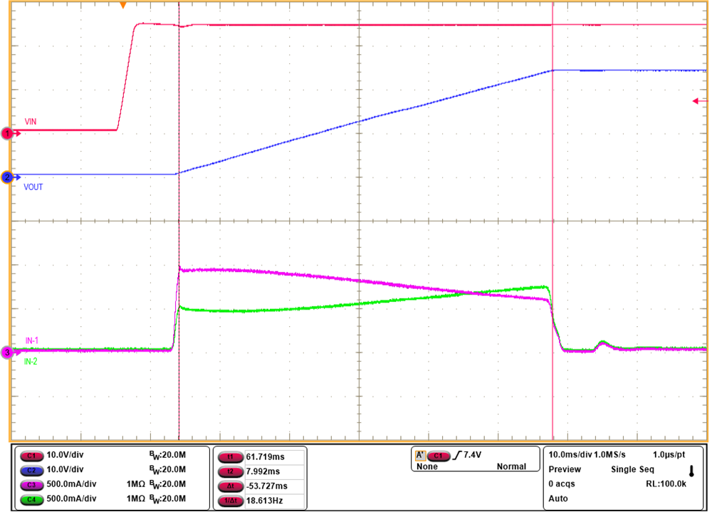
 Figure 2-2 Current Sharing Between the Devices During Start-up in dVdT mode
Figure 2-1 illustrates the circuit configuration of two TPS26631 devices in parallel. A single blocking FET Q1 on the primary eFuse is enough for reverse current blocking. Figure 2-2 shows the current sharing during start-up with dVdT pins together. Even though the ramp rate of the dVdT pin is the same for both the devices, the mismatch in the internal dVdT gain and the internal FET characteristics leads to unequal current sharing during start-up. For uniform current distribution while starting up into large loads, current limited start-up is recommended as follows
- Leave dVdT pins OPEN
- Use RILIM resistor switch network at the ILIM pin. The RILIM_Low sets the inrush current. After successful start-up, PGOOD asserts high which sets the overload current limit as per (RILIM_Low || RILIM_High) at the ILIM pin
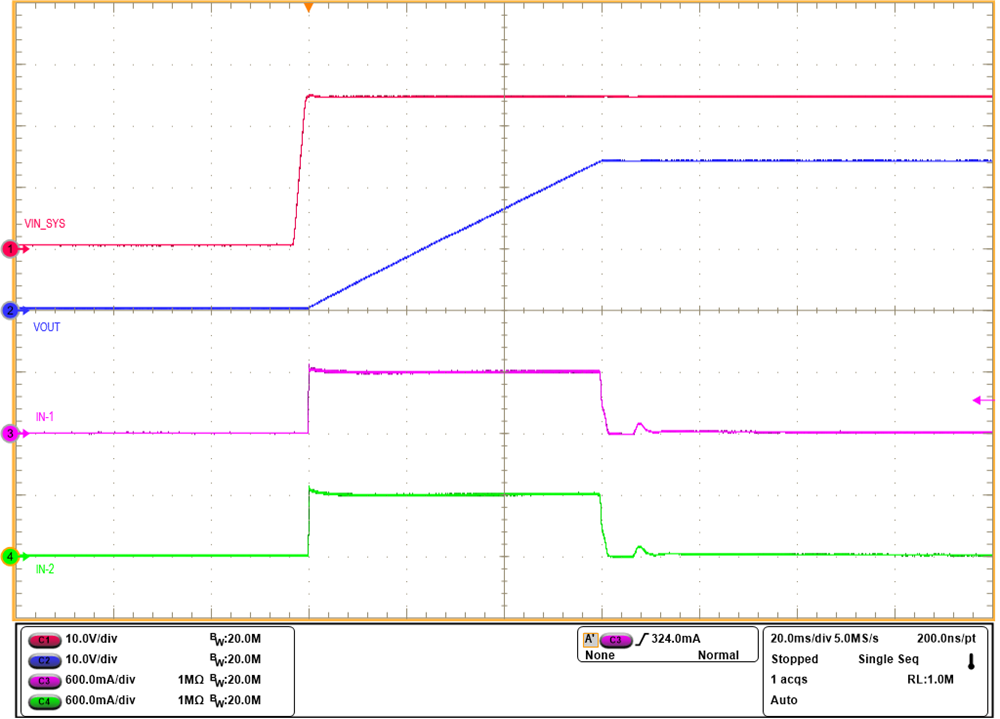
The modified parallel circuit configuration is illustrated in Figure 2-3 and the corresponding start-up waveform demonstrating equal start-up current between two TPS26631 devices is shown in Figure 2-4. In this application report, RILIM resistor switch network is considered in the design example as it ensures uniform current sharing under all the stressful events.
 Figure 2-4 Current Sharing Between the Devices During Start-up in Current-Limit
Mode