SLVAFH1A December 2022 – December 2023 TPS62933 , TPS62933F , TPS62933O , TPS62933P
- 1
- Create an Inverting Power Supply Using a TPS6293x Buck Converter With Internal Compensation
- Trademarks
- 1Configuring the Buck Converter for Inverting Buck-Boost Topology Application
- 2Choosing the Correct Buck Converter for Inverting Power Application
- 3Selecting Applicable External Components for Inverting Power Application
- 4Experimental Results
- 5Summary
- 6References
- 7Revision History
2.3 Output Current Range
In the buck configuration, the average inductor current equals the average output current because the inductor always supplies current to the load during both the on and off times of the control MOSFET. However, in the inverting buck boost configuration, the load is supplied with current only from the output capacitor and is completely disconnected from the inductor during the on time of the control MOSFET. During the off time, the inductor connects to both the output capacitor and the load (see Figure 1-3).
The peak current of the MOSFET and inductor can easily be calculated, as follows in Equation 1, Equation 2, Equation 3, and Equation 4.
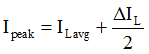
Where:
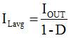
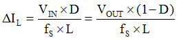
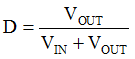
When VIN is increased and VOUT is kept constant, the duty cycle, D, and ILavg decrease, while ΔIL increases. You can see that the sum of ILavg and ΔIL decreases. So, when VIN is at the minimum, you can get the maximum Ipeak. You must choose an applicable inductor, L, to keep the maximum Ipeak lower than the minimum current limit, Icl(min) of the device. Therefore, you get Equation 5, as follows:
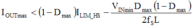
You can get the IOUTmax versus Lmin graph of the TPS6293x device, shown in Figure 4. For the TPS62933 device, Ilim_HS = 4.2 A and choose fs = 500 kHz. From Figure 4, you can see that by increasing the inductor and VINmin, or decreasing the output voltage level, this device can hold more output current in the buck-boost application.
 Figure 2-1 Output Current Range Versus
Inductor L
Figure 2-1 Output Current Range Versus
Inductor L