SLVAFJ0 april 2023 TPS650350-Q1 , TPS650352-Q1
4 Design Considerations
Automotive camera modules are typically as small as possible to support placement in remote regions of the vehicle. A designer may need to sacrifice some layout best practices in terms of conducted and radiated emissions in order to meet stringent size constraints. The SSC feature of the TPS650350-Q1 allows for a sub-optimal layout while still passing CISPR-25 emissions testing specifications.
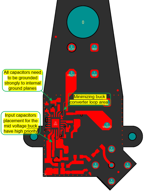
Design considerations for this layout to reduce emissions include:
- Minimize the loop area between the buck converter input capacitors and the thermal pad of the PMIC. Smaller decoupling capacitors are placed closer to the device pins.
- Minimize the loop area between the input capacitor, output inductor, and output capacitor of each buck converter.
- The mid-voltage buck converter (Buck 1) has the highest priority for external component placement on the PCB.
- The input capacitors for the low-voltage buck converters (Buck 2 and Buck 3) have the next highest placement priority.
- External components for the less EMI critical converter can be placed on the opposite side. In this case the less critical converter is Buck 2 because it has a higher output voltage (1.8 V).
- Incorporate multiple solid ground planes with low impedance connections to the ground pours on the external component layers.
 Figure 4-1 Top Layer - Zoom