SLVAFJ8 may 2023 TPS7H5001-SP
3 Test Results
 Figure 3-1 Efficiency vs. Current
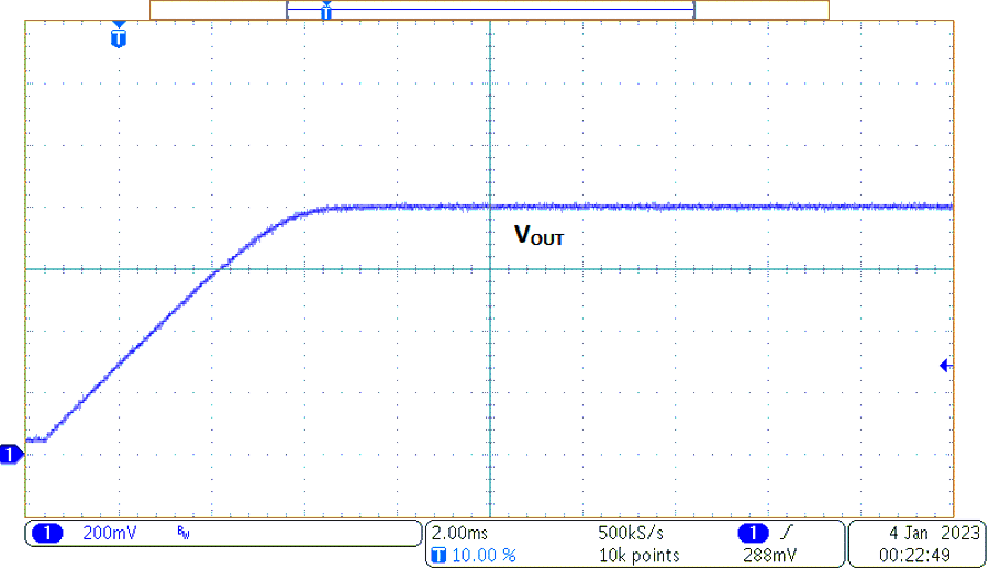
 Figure 3-2 Start-up Loaded (30 A)
Figure 3-2 shows start-up of the converter when unloaded.
 Figure 3-3 Shutdown
Figure 3-3 shows shutdown of the converter when loaded with 30 A on the output current.
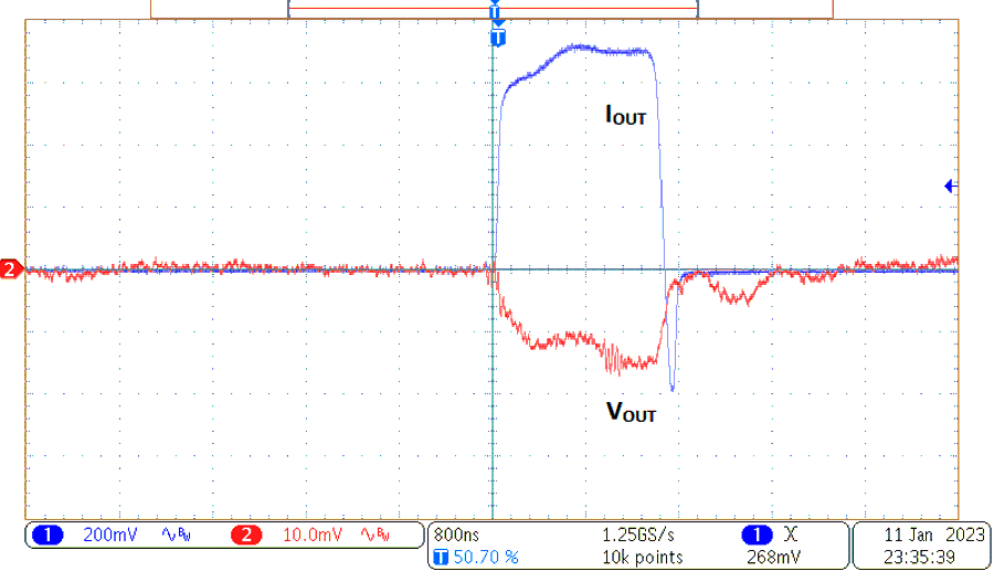
 Figure 3-4 Voltage Transient
Figure 3-4 shows the output voltage dip of the converter to a 33 A output current transient. The output current is measured across a 0.01 Ohm resistor that a FET is pulsing the current through.
 Figure 3-5 Thermal Image of Board with 80
A Output Current
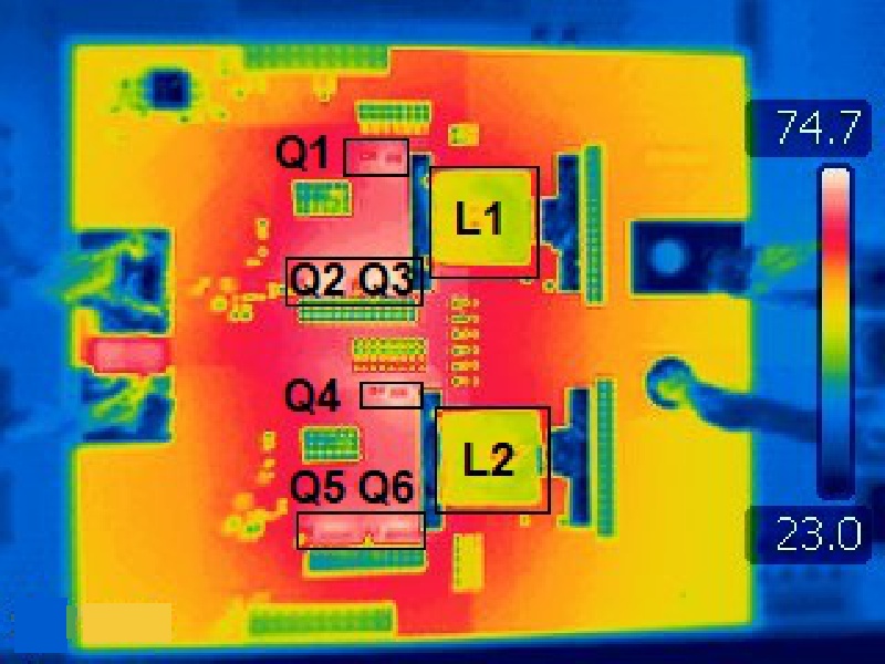
Figure 3-5 Thermal Image of Board with 80
A Output CurrentFigure 3-5 shows the thermal image of the board with 80 A of output current.
 Figure 3-6 Switch Node Voltage with Full
Output Current
Figure 3-6 Switch Node Voltage with Full
Output CurrentFigure 3-6 shows the maximum voltage on the switch node of the converter with an output current of 80 A.