SLVAFL5 September 2023 TPS61299
- 1
- Abstract
- Trademarks
- 1Introduction of Water Heater
- 2Low Voltage Start-up Boost Converter Introduction
- 3TPS61299 Ultra-low Voltage Start-up Design
- 4Ultra-low Voltage Start-up Design
- 5Summary
- 6References
3.2 The Way AVIN influence Start-up Process
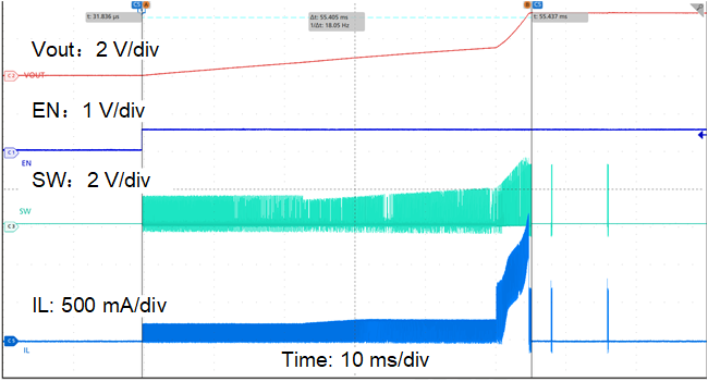
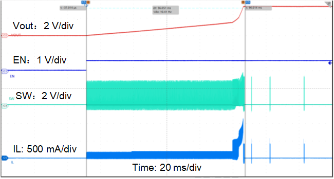
Table 3-2 shows the start-up time △T varies with different AVIN, with VOUT =3.3 V, PVIN = 150 mV and L =1 uH. △T is the time when VOUT ramps from 10% to 90% of the target voltage. With the increase of AVIN, the startup time is reduced gradually.
| AVIN (V) | △T(ms) |
|---|---|
| 0.7 | 55.4 |
| 1 | 81.6 |
| 1.2 | 88.6 |
| 1.5 | 92.8 |
| 2 | 96.1 |
| 3 | 244 |
Figure 3-2 and Figure 3-3 shows the start-up process with AVIN=0.7 V and 2 V ,with PVIN= 150 mV, VOUT=3.3 V, L=1uH. As is seen, the start-up process is faster with AVIN = 0.7 V. The start-up time varies under the two set-ups is mainly because the Down Mode period. The difference resulting from various AVIN is because the internal block should detect the AVIN and compare it with Vout to decide whether to exit down mode or enter Boost mode.
 Figure 3-2 Start-up Waveform with
AVIN = 0.7 V
 Figure 3-3 Start-up Waveform with
AVIN = 2 V
Figure 3-3 Start-up Waveform with
AVIN = 2 VIn the initial stage as shown in Figure 2-3, when Vin is higher than Vout, the TPS61299 enters Down Mode, which schematic can been seen in Figure 2-4. Afterwords, the device exits down mode and enters BOOST Mode until VOUT ramps to AVIN. The lower AVIN is , the earlier the device exits down mode operation and enters boost operation. While under boost mode the efficiency is much higher because the high side MOSFET fully turns on other than works in saturation area, which means more energy can be converted to output thus the converter could regulate to target VOUT sooner.
Under down mode, during the Ton period, the Low side MOSFET turns on and the inductor current ramps up; during the Toff period, the Low side MOSFET turns off and High side MOSFET turns on in turn. According to the volt-second balance principle of inductor, the differentiation of inductor in Equation 1 and Equation 2:
During Ton period:
During the Toff period:
The Ton period is much the same under the two cases because the PVIN is both 150 mV. While during Toff period, the voltage drop across inductor varies since the SW node voltage differs under different AVIN. The SW node voltage varies for that the source node of high side PMOS is charged to AVIN+Vgs(th), as a result of PMOS internal Cgs. Figure 3-4 shows the inductor current with AVIN=2 V and 0.7 V , the off time is much longer with AVIN=0.7V.
 Figure 3-4 Inductor Current with
Different AVIN
Figure 3-4 Inductor Current with
Different AVINIn summary, the recommendation is to choose lower AVIN to achieve ultra low VIN start-up. However, AVIN must be higher than UVLO of TPS61299, which means the minimum AVIN is 0.7 V.