SLVAFV2 June 2024 LMR51610 , TPS629210
3 Voltage Drop Comparison Between Calculation, Simulation, and Measurement
Based on the typical number in the data sheet, this section compares the voltage drop between the calculation, simulation and actual measurement. Table 3-1 shows the specifications of the TPS629210.
| Parameter | Value | Unit |
|---|---|---|
| Input Voltage | 5 | V |
| Output Voltage | 5(Ideally) | V |
| Output Current | 0.1-0.9 | A |
| Duty Cycle | 100 | % |
| High-side Resistance | 250 | mΩ |
| Low-side Resistance | 85 | mΩ |
| Inductor DC resistor | 37 | mΩ |
Table 3-2 shows the actual measurement results of TPS629210.
| Input voltage(V) | Input current(A) | Output Voltage(V) | Output Current(A) | Voltage drop(V) |
|---|---|---|---|---|
| 4.9691 | 0.0956 | 4.9386 | 0.0980 | 0.0305 |
| 4.9667 | 0.1946 | 4.9046 | 0.1972 | 0.0621 |
| 4.9645 | 0.2932 | 4.8710 | 0.2968 | 0.0935 |
| 4.9621 | 0.3927 | 4.8365 | 0.3952 | 0.1256 |
| 4.9598 | 0.4932 | 4.8017 | 0.4929 | 0.1581 |
| 4.9574 | 0.5925 | 4.7660 | 0.5920 | 0.1914 |
| 4.9551 | 0.6925 | 4.7295 | 0.6915 | 0.2256 |
| 4.9528 | 0.7920 | 4.6918 | 0.7910 | 0.2610 |
| 4.9505 | 0.8900 | 4.6527 | 0.8890 | 0.2978 |
Then, using Equation 7, we can simply calculate the voltage drop, or we can use Equation 8 to calculate by setting D equal to 1. For a more detailed comparison, a simulation model is made in plecs. Relevant parameters, such as resistance, duty cycle, and output resistor, were embedded into the model.
Table 3-3 summarizes the voltage drops based on the calculations, simulations, and real tests. To compare the deviations of the calculation and simulation from the actual parameters, the parameters used in the calculation and simulation were consistent with the actual test values.
| Output current(A) | Calculation(V) | Simulation(V) | Test(V) |
|---|---|---|---|
| 0.1 | 0.0283 | 0.0283 | 0.0305 |
| 0.2 | 0.0566 | 0.0563 | 0.0621 |
| 0.3 | 0.0853 | 0.0854 | 0.0935 |
| 0.4 | 0.1137 | 0.1137 | 0.1256 |
| 0.5 | 0.1419 | 0.1420 | 0.1581 |
| 0.6 | 0.1706 | 0.1731 | 0.1914 |
| 0.7 | 0.1996 | 0.2020 | 0.2256 |
| 0.8 | 0.2286 | 0.2286 | 0.2610 |
| 0.9 | 0.2573 | 0.2574 | 0.2978 |
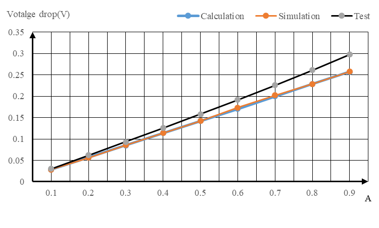 Figure 3-1 Voltage Drop Comparison of TPS629210
| Parameter | Value | Unit |
|---|---|---|
| Input Voltage | 5 | V |
| Output Voltage | 5(Ideally) | V |
| Output Current | 0.1-0.9 | A |
| Duty Cycle | 98%(Ideal) | % |
| High-side Resistance | 700 | mΩ |
| Low-side Resistance | 360 | mΩ |
| Inductor DC resistor | 137 | mΩ |
| Input voltage(V) | Input current(A) | Output Voltage(V) | Output Current(A) | Voltage drop(V) |
|---|---|---|---|---|
| 5.3889 | 0.0905 | 5.0799 | 0.1004 | 0.309 |
| 5.3865 | 0.1852 | 4.9827 | 0.1991 | 0.4038 |
| 5.3842 | 0.2812 | 4.8860 | 0.2988 | 0.4982 |
| 5.3820 | 0.3762 | 4.7851 | 0.3976 | 0.5969 |
| 5.3797 | 0.4698 | 4.6770 | 0.4949 | 0.7027 |
| 5.3774 | 0.5650 | 4.5594 | 0.5950 | 0.818 |
| 5.3752 | 0.6605 | 4.4293 | 0.6945 | 0.9459 |
| 5.3729 | 0.7540 | 4.2773 | 0.7945 | 1.0956 |
| 5.3708 | 0.8510 | 4.0572 | 0.8930 | 1.3136 |
| Output current(A) | Calculation(V) | Simulation(V) | Test(V) |
|---|---|---|---|
| 0.1 | 0.3118 | 0.3089 | 0.3090 |
| 0.2 | 0.3961 | 0.3905 | 0.4038 |
| 0.4 | 0.5669 | 0.5560 | 0.5969 |
| 0.5 | 0.6522 | 0.6388 | 0.7027 |
| 0.6 | 0.7413 | 0.7254 | 0.818 |
| 0.7 | 0.8326 | 0.8142 | 0.9459 |
| 0.8 | 0.9290 | 0.9080 | 1.0956 |
| 0.9 | 1.0381 | 1.0145 | 1.3136 |
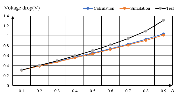 Figure 3-2 Voltage Drop Comparison of LMR51610
For the voltage drop in TPS629210, based on Table 3-2, Table 3-6, and Figure 3-1 we can see that the calculation based on Equation 5 is very close to the simulation results, but there is some deviation from the real test results.
With an increase in the output current, the deviation gradually increases. The maximum value was 0.0404V or 40.4mV. This is close to the calculation and simulation results. The reason for this deviation is the MOSFET temperature offset and practical resistance of the MOSFET and RL.
- Practical resistance of MOSFET and RL
In the calculation, we calculated the voltage drop using the typical conduction resistance in the data sheet. 250mOhm for TPS629210 and 37mΩ for the inductor used in EVM, but the practical resistance can not be very accurated 250mΩ and 37mΩ.
- Rdson Temperature offset of FETs
Based on the ATE characterization data, Rdson of the internal FET has a deviation range based on the typical value over temperature. When the voltage increased, Rdson of the FET also increased. This introduced an additional voltage drop and let the curve exhibit a certain degree of nonlinearity.
For LMR51610, as shown in Table 3-6 and Figure 3-1, the calculation and simulation results also maintain high consistency. Deviation and nonlinearity are also caused by the aforementioned issue. However, the test results of LMR51610 showed more nonlinearity because the resistances of the FETs and inductor were higher and caused a greater temperature increasement than that of TPS629210.
In addition, for LMR51610, the typical number of maximum duty cycle is 98%, but in real tests, the duty cycle has some differences, and the maximum duty cycle can be calculated using the equation in the data sheet. In this test, the duty cycle was 96% and decreased to 95.72% when the output current increase from 0.1A to 0.9A as we can see from the Period and Minimum Off Time in LMR51610, Period. But the good thing is that the practical duty cycle is close to the calculated duty cycle based on Equation 8.
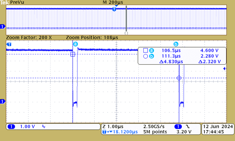 Figure 3-3 Period and Minimum Off Time in LMR51610, Period
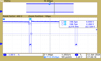 Figure 3-4 Period and Minimum Off Time in LMR51610, Off time
Therefore, by considering the effect of temperature on Rdson, the calculated results can be made more accurate. In the TPS629210EVM, there is difficulty to estimate the junction temperature increase caused by the inductor, which is related to the layout, PCB material, and copper thickness. Therefore, we mainly considered the temperature raising caused by the FETs. We can calculate the temperature raising by the power loss and effective junction to ambient resistor by reading the data sheet or the EVM guideline. Equation 9 shows the equation to calculate the temperature raising.
Where:
- Tj is the practical temperature
- TA is the room temperature
- RθJA is the effective room to ambient resistor
After Tj is obtained, Rdson can also be obtained at a specific temperature. If the relationship between temperature and Rdson is not given in data sheet, we can use experience equation to estimate the Rdson. Normally, Rdson at 150 °C is twice as high as that at 25 °C.
Table 3-7 and Figure 3-5 is the comparison table between calculated voltage drop after considering the temperature raising and practical test results. The RθJA is 60℃/W for TPS629210EVM and the Rdson is 275mΩ
| Output current(A) | Tj(℃) | Rdson(mΩ) | Calculation(V) | Test(V) |
|---|---|---|---|---|
| 0.1 | 25.151 | 275 | 0.0307 | 0.0305 |
| 0.2 | 25.642 | 276 | 0.0617 | 0.0621 |
| 0.3 | 26.453 | 277 | 0.0932 | 0.0935 |
| 0.4 | 27.577 | 278 | 0.1247 | 0.1256 |
| 0.5 | 29.009 | 280 | 0.1564 | 0.1581 |
| 0.6 | 30.783 | 282 | 0.1891 | 0.1914 |
| 0.7 | 32.890 | 284 | 0.2226 | 0.2256 |
| 0.8 | 35.320 | 287 | 0.2570 | 0.2610 |
| 0.9 | 43.150 | 291 | 0.2920 | 0.2978 |
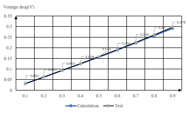 Figure 3-5 Comparison Between Calculation
and Test in TPS629210 (Add Temperature Influence)
Figure 3-5 Comparison Between Calculation
and Test in TPS629210 (Add Temperature Influence)| Output current(A) | Tj(℃) | Rdson(mΩ) | Rdson_Low(mΩ) | Calculation(V) | Test(V) |
|---|---|---|---|---|---|
| 0.1 | 25.656 | 704 | 362 | 0.3218 | 0.3090 |
| 0.2 | 27.580 | 714 | 367 | 0.4085 | 0.4038 |
| 0.3 | 30.811 | 733 | 377 | 0.5004 | 0.4982 |
| 0.4 | 35.280 | 758 | 390 | 0.5979 | 0.5969 |
| 0.5 | 40.944 | 789 | 406 | 0.7029 | 0.7027 |
| 0.6 | 48.042 | 829 | 426 | 0.8210 | 0.818 |
| 0.7 | 56.393 | 876 | 450 | 0.9516 | 0.9459 |
| 0.8 | 66.084 | 930 | 478 | 1.0991 | 1.0956 |
| 0.9 | 76.902 | 991 | 509 | 1.2726 | 1.3136 |
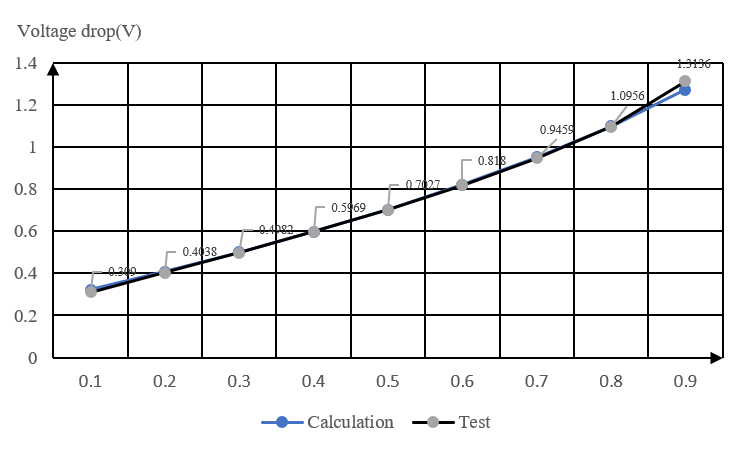 Figure 3-6 Comparison Between Calculation
and Test in LMR51610(Add Temperature Influence)
Figure 3-6 Comparison Between Calculation
and Test in LMR51610(Add Temperature Influence)As shown in the results, once adding the temperature influence on the resistance of the FET, the calculation results were more accurate.