SLVAFZ0 November 2024 DRV8161 , DRV8162
3.2.1.1 MOSFET Placement
With the availability of three separate half-bridges you now have the option to place the IC close to the MOSFETs for that phase. This improves signal integrity and reduces parasitics on the gate and source nodes.
- Source node transients or ringing:
Shorter gate or source paths between the driver and the MOSFET can help dampen the effects of trace inductance. This can help reduce the effects of source node ringing and improve EMI performance by effectively decreases the total loop inductance.
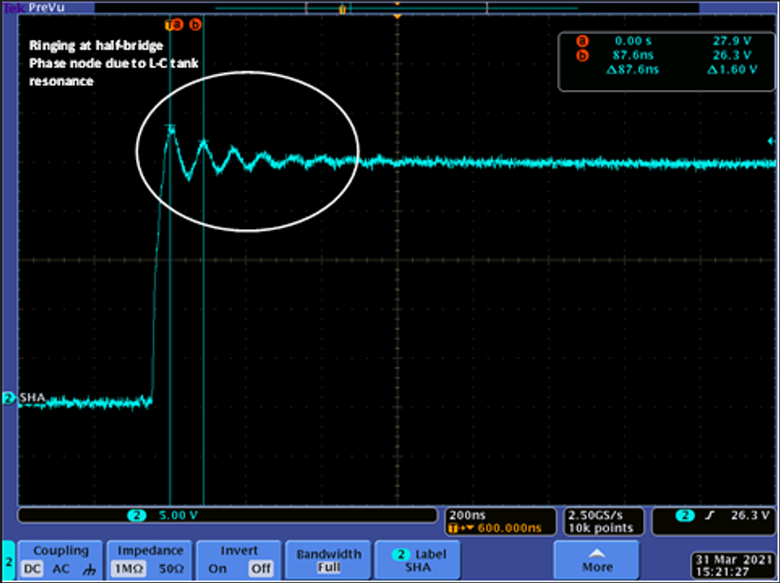
With lower effects of parasitics, you can also expect to see smaller source dips or transients. Figure 3-2 shows the ringing one can see at phase voltage switching
 Figure 3-2 Motor Driver Phase Output Waveform Showing Ringing
- Signal Integrity:
Any signal from the motor power stage that gets measured from the driver can offer benefits when the path between the origin of the signal to the measurement site gets reduced (Figure 3-3).
Current flow being sensed by the driver across the shunt resistor can be more accurate since the CSA is physically closer to the sense resistor.
Similarly, the VDS measurement for overcurrent protection is measured at the driver gate and source pins. So, if there is a large difference in drain to source between the driver and the FET, the VDS monitor is not accurate. Therefore, having the MOSFET and driver closer can result in smaller parasitic inductance helping reduce overshoot or ringing of gate signal.
Figure 3-3 Impact of MOSFET placement on signal integrity