SLVS238L August 1999 – November 2024 TL331 , TL331B , TL391B
PRODUCTION DATA
- 1
- 1 Features
- 2 Applications
- 3 Description
- 4 Pin Configuration and Functions
-
5 Specifications
- 5.1 Absolute Maximum Ratings, TL331 and TL331K
- 5.2 Absolute Maximum Ratings, TL331B and TL391B
- 5.3 ESD Ratings - TL331B and TL391B
- 5.4 ESD Ratings, TL331 and TL331K
- 5.5 Recommended Operating Conditions, TL331B and TL391B
- 5.6 Recommended Operating Conditions, TL331 and TL331K
- 5.7 Thermal Information
- 5.8 Electrical Characteristics, TL331B and TL391B
- 5.9 Switching Characteristics, TL331B and TL391B
- 5.10 Electrical Characteristics, TL331 and TL331K
- 5.11 Switching Characteristics, TL331 and TL331K
- 5.12 Typical Characteristics
- 6 Detailed Description
- 7 Application and Implementation
- 8 Device and Documentation Support
- 9 Revision History
- 10Mechanical, Packaging, and Orderable Information
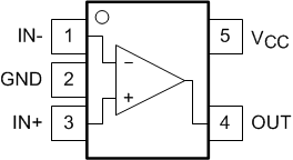
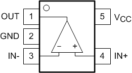
4 Pin Configuration and Functions

Note reversed inputs compared to similar common pinout
Figure 4-1 TL331, TL331B DBV Package, 5-Pin SOT-23, Top View
Note reversed inputs compared to similar common pinout
Figure 4-2 TL391B DBV Package, 5-Pin SOT-23, Top View