SLVS503F November   2003  – February 2020 TPS2490 , TPS2491

PRODUCTION DATA.  

  1. Features
  2. Applications
  3. Description
    1.     Device Images
      1.      Typical Application
  4. Revision History
  5. Pin Configuration and Functions
    1.     Pin Functions
  6. Specifications
    1. 6.1 Absolute Maximum Ratings
    2. 6.2 ESD Ratings
    3. 6.3 Recommended Operating Conditions
    4. 6.4 Thermal Information
    5. 6.5 Electrical Characteristics
    6. 6.6 Switching Characteristics
    7. 6.7 Typical Characteristics
  7. Detailed Description
    1. 7.1 Overview
    2. 7.2 Functional Block Diagram
    3. 7.3 Feature Description
      1. 7.3.1  VCC
      2. 7.3.2  SENSE
      3. 7.3.3  GATE
      4. 7.3.4  OUT
      5. 7.3.5  EN
      6. 7.3.6  VREF
      7. 7.3.7  PROG
      8. 7.3.8  TIMER
      9. 7.3.9  PG
      10. 7.3.10 GND
    4. 7.4 Device Functional Modes
      1. 7.4.1 Board Plug-In ()
      2. 7.4.2 TIMER and PG Operation ()
      3. 7.4.3 Action of the Constant Power Engine ()
      4. 7.4.4 Response to a Hard Output Short ( and )
      5. 7.4.5 Automatic Restart ()
  8. Application and Implementation
    1. 8.1 Application Information
      1. 8.1.1 Alternative Inrush Designs
        1. 8.1.1.1 Gate Capacitor (dV/dt) Control
        2. 8.1.1.2 PROG Inrush Control
      2. 8.1.2 Additional Design Considerations
        1. 8.1.2.1 Use of PG
        2. 8.1.2.2 Faults and Backplane Voltage Droop
        3. 8.1.2.3 Output Clamp Diode
        4. 8.1.2.4 Gate Clamp Diode
        5. 8.1.2.5 High Gate Capacitance Applications
        6. 8.1.2.6 Input Bypass
        7. 8.1.2.7 Output Short Circuit Measurements
    2. 8.2 Typical Application
      1. 8.2.1 Design Requirements
      2. 8.2.2 Detailed Design Procedure
        1. 8.2.2.1 Select RSNS and CL setting
        2. 8.2.2.2 Selecting the Hot Swap FET(s)
        3. 8.2.2.3 Select Power Limit
        4. 8.2.2.4 Set Fault Timer
        5. 8.2.2.5 Check MOSFET SOA
        6. 8.2.2.6 Set Under-Voltage Threshold
        7. 8.2.2.7 Choose R5, and CIN
        8. 8.2.2.8 Input and Output Protection
        9. 8.2.2.9 Final Schematic and Component Values
      3. 8.2.3 Application Curves
  9. Power Supply Recommendations
  10. 10Layout
    1. 10.1 Layout Guidelines
      1. 10.1.1 PC Board Guidelines
      2. 10.1.2 System Considerations
    2. 10.2 Layout Example
  11. 11Device and Documentation Support
    1. 11.1 Development Support
    2. 11.2 Documentation Support
      1. 11.2.1 Related Documentation
    3. 11.3 Related Links
    4. 11.4 Receiving Notification of Documentation Updates
    5. 11.5 Community Resources
    6. 11.6 Trademarks
    7. 11.7 Electrostatic Discharge Caution
    8. 11.8 Glossary
  12. 12Mechanical, Packaging, and Orderable Information

Typical Characteristics

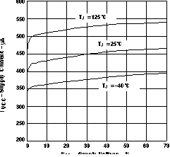
TPS2490 TPS2491 icc_v_vcc_lvs503.gifFigure 1. Supply Current vs Supply Voltage
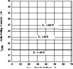
TPS2490 TPS2491 igtup_v_vcc_lvs503.gifFigure 3. Gate Pullup Current vs Supply Voltage
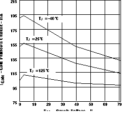
TPS2490 TPS2491 igtdn2_v_vcc_lvs503.gifFigure 5. Gate Pulldown Current vs Supply Voltage (EN = 4 V, V(VCC – Sense) = 200 mV)
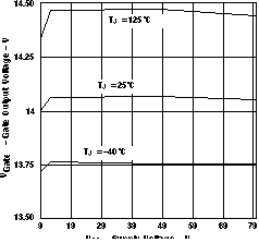
TPS2490 TPS2491 vgate_vcc_lvs503.gifFigure 7. Gate Output Voltage vs Supply Voltage
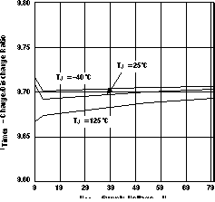
TPS2490 TPS2491 Itimer_Chrg_lvs503.gifFigure 9. Timer Charge/Discharge Ratio vs Supply Voltage and Temperature
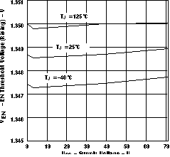
TPS2490 TPS2491 VenR_Vcc_lvs503.gifFigure 11. EN Threshold Voltage (Rising) vs Supply Voltage
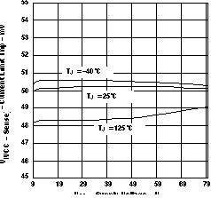
TPS2490 TPS2491 vccse_v_vcc_lvs503.gifFigure 2. Current Limit Trip vs Supply Voltage
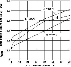
TPS2490 TPS2491 igtdn_v_vcc_ivs503.gifFigure 4. Gate Pulldown Current (EN = 0 V) vs Supply Voltage
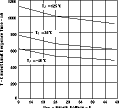
TPS2490 TPS2491 Ilim_resp_lvs503.gifFigure 6. Current Limit Response Time vs Supply Voltage (EN = 4 V, V(VCC – Sense) = 200 mV)
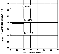
TPS2490 TPS2491 Itimer_vcc_lvs503.gifFigure 8. Timer Pullup Current vs Supply Voltage
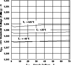
TPS2490 TPS2491 Ven_vcc_lvs503.gifFigure 10. EN Threshold Voltage (Falling) vs Supply Voltage
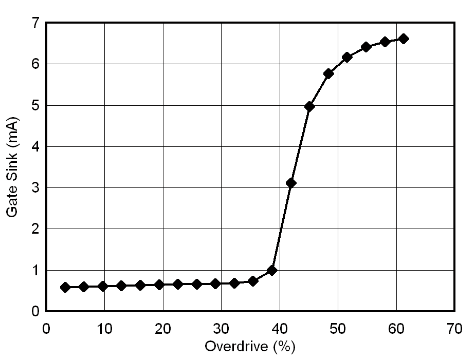
TPS2490 TPS2491 D001_SLVS503.gifFigure 12. Gate Sink vs Overdrive Measurements