TPS2292x 3.6-V, 2-A, 14-mΩ ON-Resistance Load Switch With Controlled Turnon
1 Features
- Integrated P-Channel Load Switch
- Input Voltage: 0.9 V to 3.6 V
- ON-Resistance (Typical Values)
- rON = 14 mΩ at VIN = 3.6 V
- rON = 20 mΩ at VIN = 2.5 V
- rON = 33 mΩ at VIN = 1.8 V
- rON = 67 mΩ at VIN = 1.2 V
- rON = 116 mΩ at VIN = 1.0 V
- 2-A Maximum Continuous Switch Current
- Quiescent Current:
- Typical 78 nA at 1.8 V
- Shutdown Current:
- Typical 35 nA at 1.8 V
- Low Threshold Control Input Enable the use of
1.2 V, 1.8 V, 2.5 V, or 3.3 V Logic - Controlled Slew Rate to Avoid Inrush Currents
- tR = 30 μs at VIN = 1.8 V (TPS22921/2)
- tR = 200 μs at VIN = 1.8 V (TPS22922B)
- Quick Output Discharge (TPS22922/2B)
- ESD Performance Tested Per JESD 22
- 3000-V Human Body Model
(A114-B, Class II) - 1000-V Charged-Device Model (C101)
- 3000-V Human Body Model
- Six Terminal Wafer-Chip-Scale DSBGA Package (nominal dimensions shown - see Mechanical, Packaging, and Orderable Information for details)
2 Applications
- PDAs
- Cell Phones
- GPS Devices
- MP3 Players
- Peripheral Ports
- Portable Media Players
- RF Modules
3 Description
TPS22921, TPS22922, and TPS22922B are small, low rON load switches with controlled turnon. The TPS22921/2/2B contains a P-channel MOSFET that can operate over an input voltage range of 0.9 V to 3.6 V. The switch is controlled by an on/off input (ON), which can interface directly with low-voltage control signals. In TPS22922 and in TPS22922B, a 65-Ω on-chip load resistor is added for output quick discharge when the switch is turned off. The rise time (slew rate) of the device is internally controlled in order to avoid inrush current: TPS22921 and TPS22922 feature a 30-μs rise time, whereas TPS22922B is 200 μs.
TPS22921, TPS22922, and TPS22922B feature low quiescent and shutdown currents and are available in space-saving 6-pin wafer-chip-scale packages DSBGA (WCSP: YZP and YZT with 0.5-mm pitch and YFP with 0.4-mm pitch) which make them ideal for portable electronics. The devices are characterized for operation over the free-air temperature range of –40°C to 85°C.
Device Information(1)
| PART NUMBER | PACKAGE | BODY SIZE (NOM) |
|---|---|---|
| TPS22921(1) | YZT | 0.9 mm × 1.4 mm |
| YZP | ||
| YFP | 0.8 mm × 1.2 mm | |
| TPS22922 TPS22922B |
YZP | 0.9 mm × 1.4 mm |
| YFP | 0.8 mm × 1.2 mm |
- For all available packages, see the orderable addendum at the end of the data sheet.
5 Revision History
Changes from B Revision (May 2012) to C Revision
- Added Pin Configuration and Functions section, ESD Rating table, Feature Description section, Device Functional Modes, Application and Implementation section, Power Supply Recommendations section, Layout section, Device and Documentation Support section, and Mechanical, Packaging, and Orderable Information section Go
Changes from A Revision (December 2008) to B Revision
- Changed Feature From: Ultra-Low Quiescent Current: 78 nA at 1.8 V To: Ultra-Low Quiescent Current: Typical 78 nA at 1.8 VGo
- Changed Feature From: Typical 78 nA at 1.8 V To: Ultra-Low Shutdown Current: Typical 35 nA at 1.8 VGo
- Changed Feature From: Six Terminal Wafer-Chip-Scale Package To: Six Terminal Wafer-Chip-Scale Package (nominal dimensions shown - see addendum for detailsGo
- Changed Feature From: 0.5-mm Height To: 0.5-mm Height (YFP)Go
- Changed TPS22921 QUICK OUTPUT DISCHARGE From: - To: NoGo
- Changed the format of the ELECTRICAL CHARACTERISTICS Test Conditions From: VIN = 1-V to VIN = 1 VGo
- Deleted Note 1 - RL_CHIP = 120 Ω from all SWITCHING CHARACTERISTICS tablesGo
- Changed Figure 50 title From: tOFF Response To: tON ResponseGo
Changes from * Revision (November 2008) to A Revision
- Added Note A to the TYPICAL APPLICATION circuitGo
6 Device Comparison Table
| RON AT 1.8 V (TYP) |
RISE TIME (TYP at 1.8 V) |
QUICK OUTPUT DISCHARGE(1) |
MAX OUTPUT CURRENT |
ENABLE | |
|---|---|---|---|---|---|
| TPS22921 | 33 mΩ | 30 μs | No | 2 A | Active high |
| TPS22922 | 33 mΩ | 30 μs | Yes | 2 A | Active high |
| TPS22922B | 33 mΩ | 200 μs | Yes | 2 A | Active high |
7 Pin Configuration and Functions

Pin Assignments
| C | ON | GND |
| B | VIN | VOUT |
| A | VIN | VOUT |
| 2 | 1 |
Pin Functions
| PIN | I/O | DESCRIPTION | |
|---|---|---|---|
| NO. | NAME | ||
| A1 | VOUT | O | Switch output |
| A2 | VIN | I | Switch input. Use a bypass capacitor to ground (ceramic) |
| B1 | VOUT | O | Switch output |
| B2 | VIN | I | Switch input. Use a bypass capacitor to ground (ceramic) |
| C1 | GND | – | Ground |
| C2 | ON | I | Switch control input, active high. Do not leave floating |
8 Specifications
8.1 Absolute Maximum Ratings(1)
| MIN | MAX | UNIT | ||||
|---|---|---|---|---|---|---|
| VIN | Input voltage | –0.3 | 4 | V | ||
| VOUT | Output voltage | VIN + 0.3 | V | |||
| VON | Input voltage | –0.3 | 4 | V | ||
| P | Power dissipation at TA = 25°C | 0.645 | W | |||
| IMAX | Maximum continuous switch current | 2 | A | |||
| TA | Operating free-air temperature | –40 | 85 | °C | ||
| Tlead | Maximum lead temperature (10-s soldering time) | 300 | °C | |||
| Tstg | Storage temperature | –65 | 150 | °C | ||
8.2 ESD Ratings
| VALUE | UNIT | |||
|---|---|---|---|---|
| V(ESD) | Electrostatic discharge | Human body model (HBM), per ANSI/ESDA/JEDEC JS-001(1) | ±3000 | V |
| Charged-device model (CDM), per JEDEC specification JESD22-C101(2) | ±1000 | |||
| Machine model (MM) | ±300 | |||
8.3 Recommended Operating Conditions
| MIN | MAX | UNIT | ||
|---|---|---|---|---|
| VIN | Input voltage range | 0.9 | 3.6 | V |
| VOUT | Output voltage range | VIN | V | |
| VIH | High-level input voltage, ON | 0.85 | 3.6 | V |
| VIL | Low-level input voltage, ON | 0.4 | V | |
| CIN | Input capacitor | 1(1) | µF |
8.4 Thermal Information
| THERMAL METRIC(1) | TPS22921, TPS22922, TPS22922B | TPS22921 | UNIT | ||
|---|---|---|---|---|---|
| YFP | YZP | YZT | |||
| 6 PINS | |||||
| RθJA | Junction-to-ambient thermal resistance | 125.1 | 131 | 120.7 | °C/W |
| RθJC(top) | Junction-to-case (top) thermal resistance | 1.4 | 1.3 | 2.1 | |
| RθJB | Junction-to-board thermal resistance | 26 | 22.6 | 26.4 | |
| ψJT | Junction-to-top characterization parameter | 0.3 | 5.2 | 3.7 | |
| ψJB | Junction-to-board characterization parameter | 26 | 22.6 | 26.4 | |
8.5 Electrical Characteristics
VIN = 0.9 V to 3.6 V, TA = –40°C to 85°C (unless otherwise noted)| PARAMETER | TEST CONDITIONS | TA | MIN | TYP(1) | MAX | UNIT | ||
|---|---|---|---|---|---|---|---|---|
| IQ | Quiescent current | IOUT = 0 mA | VIN = 1 V | Full | 30 | 120 | nA | |
| VIN = 1.8 V | Full | 78 | 235 | |||||
| VIN = 3.6 V | Full | 200 | 880 | |||||
| IIN(OFF) | OFF-state supply current | VON = GND, OUT = Open |
VIN = 1 V | Full | 10 | 210 | nA | |
| VIN = 1.8 V | Full | 35 | 260 | |||||
| VIN = 3.6 V | Full | 120 | 700 | |||||
| IIN(LEAKAGE) | OFF-state switch current | VON = GND, VOUT = 0 V |
VIN = 1 V | Full | 12 | 140 | nA | |
| VIN = 1.8 V | Full | 50 | 230 | |||||
| VIN = 3.6 V | Full | 130 | 610 | |||||
| rON | ON-state resistance | IOUT = –200 mA | VIN = 3.6 V | 25°C | 14 | 45 | mΩ | |
| Full | 50 | |||||||
| VIN = 2.5 V | 25°C | 20 | 55 | |||||
| Full | 60 | |||||||
| VIN = 1.8 V | 25°C | 33 | 65 | |||||
| Full | 75 | |||||||
| VIN = 1.2 V | 25°C | 67 | 100 | |||||
| Full | 120 | |||||||
| VIN = 1.1 V | 25°C | 82 | 150 | |||||
| Full | 160 | |||||||
| VIN = 1 V | 25°C | 116 | 160 | |||||
| Full | 170 | |||||||
| rPD | Output pulldown resistance | VIN = 3.3 V, VON = 0 V, IOUT = 30 mA (TPS22922 and TPS22922B only) |
25°C | 65 | 120 | Ω | ||
| ION | ON input leakage current | VON = 1.1 V to 3.6 V or GND | Full | 25 | nA | |||
8.6 Switching Characteristics: VIN = 0.9 V
VIN = 0.9 V, TA = 25°C (unless otherwise noted)| PARAMETER | TEST CONDITIONS | TPS22921 | TPS22922 | TPS22922B | UNIT | ||||||||
|---|---|---|---|---|---|---|---|---|---|---|---|---|---|
| MIN | TYP | MAX | MIN | TYP | MAX | MIN | TYP | MAX | |||||
| tON | Turn-ON time | RL = 500 Ω | CL = 0.1 μF | 121 | 121 | 638 | μs | ||||||
| CL = 1 μF | 160 | 160 | 712 | ||||||||||
| CL = 3 μF | 188 | 188 | 799 | ||||||||||
| tOFF | Turn-OFF time | RL = 500 Ω | CL = 0.1 μF | 46 | 40 | 40 | μs | ||||||
| CL = 1 μF | 308 | 279 | 279 | ||||||||||
| CL = 3 μF | 975 | 807 | 807 | ||||||||||
| tr | VOUT rise time | RL = 500 Ω | CL = 0.1 μF | 60 | 60 | 462 | μs | ||||||
| CL = 1 μF | 85 | 85 | 465 | ||||||||||
| CL = 3 μF | 107 | 107 | 507 | ||||||||||
| tf | VOUT fall time | RL = 500 Ω | CL = 0.1 μF | 119 | 51 | 51 | μs | ||||||
| CL = 1 μF | 969 | 434 | 434 | ||||||||||
| CL = 3 μF | 3174 | 1264 | 1264 | ||||||||||
8.7 Switching Characteristics: VIN = 1 V
VIN = 1 V, TA = 25°C (unless otherwise noted)| PARAMETER | TEST CONDITIONS | TPS22921 | TPS22922 | TPS22922B | UNIT | ||||||||
|---|---|---|---|---|---|---|---|---|---|---|---|---|---|
| MIN | TYP | MAX | MIN | TYP | MAX | MIN | TYP | MAX | |||||
| tON | Turn-ON time | RL = 500 Ω | CL = 0.1 μF | 105 | 105 | 549 | μs | ||||||
| CL = 1 μF | 136 | 136 | 613 | ||||||||||
| CL = 3 μF | 157 | 157 | 683 | ||||||||||
| tOFF | Turn-OFF time | RL = 500 Ω | CL = 0.1 μF | 46 | 28 | 28 | μs | ||||||
| CL = 1 μF | 309 | 186 | 186 | ||||||||||
| CL = 3 μF | 983 | 511 | 511 | ||||||||||
| tr | VOUT rise time | RL = 500 Ω | CL = 0.1 μF | 51 | 51 | 386 | μs | ||||||
| CL = 1 μF | 78 | 78 | 388 | ||||||||||
| CL = 3 μF | 88 | 88 | 419 | ||||||||||
| tf | VOUT fall time | RL = 500 Ω | CL = 0.1 μF | 121 | 34 | 34 | μs | ||||||
| CL = 1 μF | 986 | 306 | 306 | ||||||||||
| CL = 3 μF | 3300 | 908 | 908 | ||||||||||
8.8 Switching Characteristics: VIN = 1.1 V
VIN = 1.1 V, TA = 25°C (unless otherwise noted)| PARAMETER | TEST CONDITIONS | TPS22921 | TPS22922 | TPS22922B | UNIT | ||||||||
|---|---|---|---|---|---|---|---|---|---|---|---|---|---|
| MIN | TYP | MAX | MIN | TYP | MAX | MIN | TYP | MAX | |||||
| tON | Turn-ON time | RL = 500 Ω | CL = 0.1 μF | 91 | 93 | 484 | μs | ||||||
| CL = 1 μF | 118 | 118 | 540 | ||||||||||
| CL = 3 μF | 137 | 137 | 599 | ||||||||||
| tOFF | Turn-OFF time | RL = 500 Ω | CL = 0.1 μF | 44 | 21 | 21 | μs | ||||||
| CL = 1 μF | 311 | 144 | 144 | ||||||||||
| CL = 3 μF | 99 | 383 | 383 | ||||||||||
| tr | VOUT rise time | RL = 500 Ω | CL = 0.1 μF | 46 | 46 | 335 | μs | ||||||
| CL = 1 μF | 60 | 60 | 336 | ||||||||||
| CL = 3 μF | 76 | 76 | 363 | ||||||||||
| tf | VOUT fall time | RL = 500 Ω | CL = 0.1 μF | 122 | 29 | 29 | μs | ||||||
| CL = 1 μF | 1000 | 224 | 224 | ||||||||||
| CL = 3 μF | 3300 | 732 | 732 | ||||||||||
8.9 Switching Characteristics: VIN = 1.2 V
VIN = 1.2 V, TA = 25°C (unless otherwise noted)| PARAMETER | TEST CONDITIONS | TPS22921 | TPS22922 | TPS22922B | UNIT | ||||||||
|---|---|---|---|---|---|---|---|---|---|---|---|---|---|
| MIN | TYP | MAX | MIN | TYP | MAX | MIN | TYP | MAX | |||||
| tON | Turn-ON time | RL = 500 Ω | CL = 0.1 μF | 83 | 83 | 435 | μs | ||||||
| CL = 1 μF | 103 | 103 | 485 | ||||||||||
| CL = 3 μF | 122 | 122 | 536 | ||||||||||
| tOFF | Turn-OFF time | RL = 500 Ω | CL = 0.1 μF | 44 | 17 | 17 | μs | ||||||
| CL = 1 μF | 312 | 117 | 117 | ||||||||||
| CL = 3 μF | 1000 | 319 | 319 | ||||||||||
| tr | VOUT rise time | RL = 500 Ω | CL = 0.1 μF | 41 | 41 | 301 | μs | ||||||
| CL = 1 μF | 54 | 54 | 302 | ||||||||||
| CL = 3 μF | 67 | 67 | 325 | ||||||||||
| tf | VOUT fall time | RL = 500 Ω | CL = 0.1 μF | 123 | 25 | 25 | μs | ||||||
| CL = 1 μF | 1000 | 214 | 214 | ||||||||||
| CL = 3 μF | 3400 | 632 | 632 | ||||||||||
8.10 Switching Characteristics: VIN = 1.8 V
VIN = 1.8 V, TA = 25°C (unless otherwise noted)| PARAMETER | TEST CONDITIONS | TPS22921 | TPS22922 | TPS22922B | UNIT | ||||||||
|---|---|---|---|---|---|---|---|---|---|---|---|---|---|
| MIN | TYP | MAX | MIN | TYP | MAX | MIN | TYP | MAX | |||||
| tON | Turn-ON time | RL = 500 Ω | CL = 0.1 μF | 54 | 54 | 282 | μs | ||||||
| CL = 1 μF | 67 | 67 | 314 | ||||||||||
| CL = 3 μF | 78 | 78 | 344 | ||||||||||
| tOFF | Turn-OFF time | RL = 500 Ω | CL = 0.1 μF | 41 | 10 | 10 | μs | ||||||
| CL = 1 μF | 312 | 67 | 67 | ||||||||||
| CL = 3 μF | 1000 | 181 | 181 | ||||||||||
| tr | VOUT rise time | RL = 500 Ω | CL = 0.1 μF | 30 | 30 | 200 | μs | ||||||
| CL = 1 μF | 37 | 37 | 202 | ||||||||||
| CL = 3 μF | 47 | 47 | 219 | ||||||||||
| tf | VOUT fall time | RL = 500 Ω | CL = 0.1 μF | 121 | 17 | 17 | μs | ||||||
| CL = 1 μF | 1000 | 158 | 158 | ||||||||||
| CL = 3 μF | 3450 | 461 | 461 | ||||||||||
8.11 Switching Characteristics: VIN = 2.5 V
VIN = 2.5 V, TA = 25°C (unless otherwise noted)| PARAMETER | TEST CONDITIONS | TPS22921 | TPS22922 | TPS22922B | UNIT | ||||||||
|---|---|---|---|---|---|---|---|---|---|---|---|---|---|
| MIN | TYP | MAX | MIN | TYP | MAX | MIN | TYP | MAX | |||||
| tON | Turn-ON time | RL = 500 Ω | CL = 0.1 μF | 40 | 40 | 211 | μs | ||||||
| CL = 1 μF | 50 | 50 | 233 | ||||||||||
| CL = 3 μF | 59 | 59 | 256 | ||||||||||
| tOFF | Turn-OFF time | RL = 500 Ω | CL = 0.1 μF | 41 | 10 | 10 | μs | ||||||
| CL = 1 μF | 316 | 56 | 56 | ||||||||||
| CL = 3 μF | 1000 | 153 | 153 | ||||||||||
| tr | VOUT rise time | RL = 500 Ω | CL = 0.1 μF | 23 | 23 | 164 | μs | ||||||
| CL = 1 μF | 29 | 29 | 165 | ||||||||||
| CL = 3 μF | 38 | 38 | 177 | ||||||||||
| tf | VOUT fall time | RL = 500 Ω | CL = 0.1 μF | 122 | 16 | 16 | μs | ||||||
| CL = 1 μF | 1086 | 147 | 147 | ||||||||||
| CL = 3 μF | 3600 | 430 | 430 | ||||||||||
8.12 Switching Characteristics: VIN = 3 V
VIN = 3 V, TA = 25°C (unless otherwise noted)| PARAMETER | TEST CONDITIONS | TPS22921 | TPS22922 | TPS22922B | UNIT | ||||||||
|---|---|---|---|---|---|---|---|---|---|---|---|---|---|
| MIN | TYP | MAX | MIN | TYP | MAX | MIN | TYP | MAX | |||||
| tON | Turn-ON time | RL = 500 Ω | CL = 0.1 μF | 30 | 30 | 182 | μs | ||||||
| CL = 1 μF | 38 | 38 | 201 | ||||||||||
| CL = 3 μF | 45 | 45 | 221 | ||||||||||
| tOFF | Turn-OFF time | RL = 500 Ω | CL = 0.1 μF | 40 | 10 | 10 | μs | ||||||
| CL = 1 μF | 353 | 51 | 51 | ||||||||||
| CL = 3 μF | 1036 | 139 | 139 | ||||||||||
| tr | VOUT rise time | RL = 500 Ω | CL = 0.1 μF | 20 | 20 | 149 | μs | ||||||
| CL = 1 μF | 25 | 25 | 150 | ||||||||||
| CL = 3 μF | 33 | 33 | 161 | ||||||||||
| tf | VOUT fall time | RL = 500 Ω | CL = 0.1 μF | 104 | 15 | 15 | μs | ||||||
| CL = 1 μF | 1030 | 143 | 143 | ||||||||||
| CL = 3 μF | 3230 | 419 | 419 | ||||||||||
8.13 Switching Characteristics: VIN = 3.6 V
VIN = 3.6 V, TA = 25°C (unless otherwise noted)| PARAMETER | TEST CONDITIONS | TPS22921 | TPS22922 | TPS22922B | UNIT | ||||||||
|---|---|---|---|---|---|---|---|---|---|---|---|---|---|
| MIN | TYP | MAX | MIN | TYP | MAX | MIN | TYP | MAX | |||||
| tON | Turn-ON time | RL = 500 Ω | CL = 0.1 μF | 30 | 30 | 159 | μs | ||||||
| CL = 1 μF | 38 | 38 | 175 | ||||||||||
| CL = 3 μF | 45 | 45 | 193 | ||||||||||
| tOFF | Turn-OFF time | RL = 500 Ω | CL = 0.1 μF | 42 | 10 | 10 | μs | ||||||
| CL = 1 μF | 310 | 51 | 51 | ||||||||||
| CL = 3 μF | 988 | 139 | 139 | ||||||||||
| tr | VOUT rise time | RL = 500 Ω | CL = 0.1 μF | 20 | 20 | 137 | μs | ||||||
| CL = 1 μF | 25 | 25 | 138 | ||||||||||
| CL = 3 μF | 33 | 33 | 148 | ||||||||||
| tf | VOUT fall time | RL = 500 Ω | CL = 0.1 μF | 120 | 15 | 15 | μs | ||||||
| CL = 1 μF | 1100 | 143 | 143 | ||||||||||
| CL = 3 μF | 3600 | 419 | 419 | ||||||||||
8.14 Typical Characteristics
8.14.1 Typical DC Characteristics
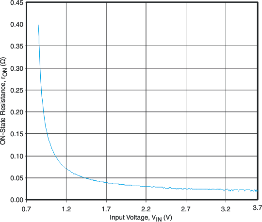 Figure 1. rON vs VIN
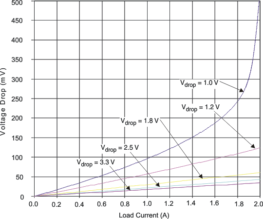 Figure 3. Voltage Drop vs Load Current
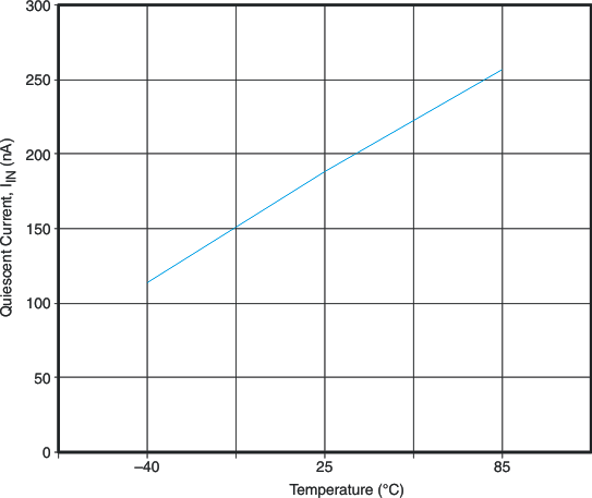 Figure 5. Quiescent Current vs Temperature
(VIN = 3.3 V, IOUT = 0 mA)
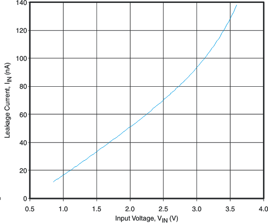 Figure 7. Leakage Current vs VIN
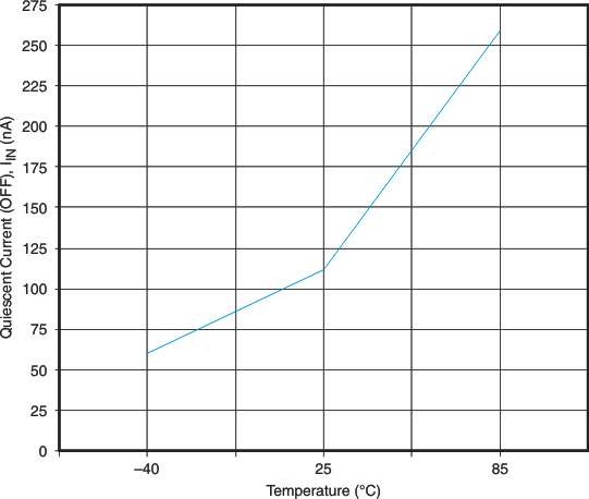 Figure 9. IIN (OFF) vs Temperature (VIN = 3.3 V)
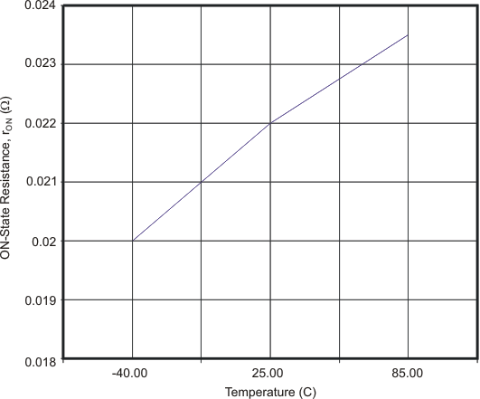 Figure 2. rON vs Temperature (VIN = 3.3 V)
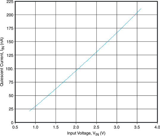 Figure 4. Quiescent Current vs VIN (VON = VIN)
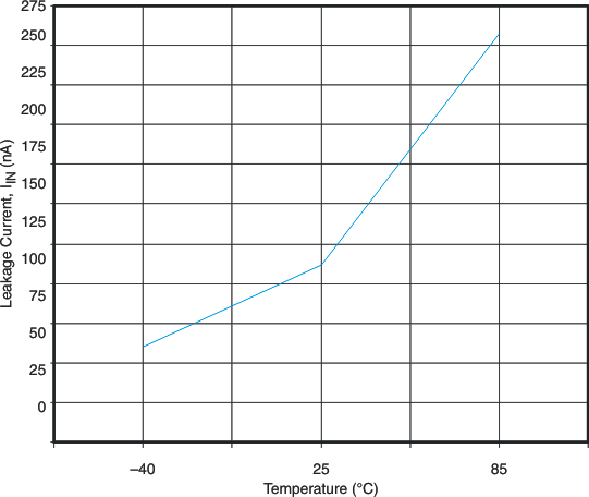 Figure 6. IIN Leakage Current vs Temperature (VIN = 3.3 V)
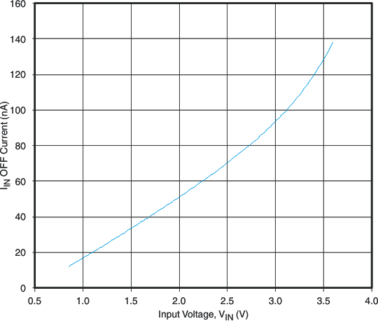 Figure 8. IIN (OFF) vs VIN (VON = 0 V)
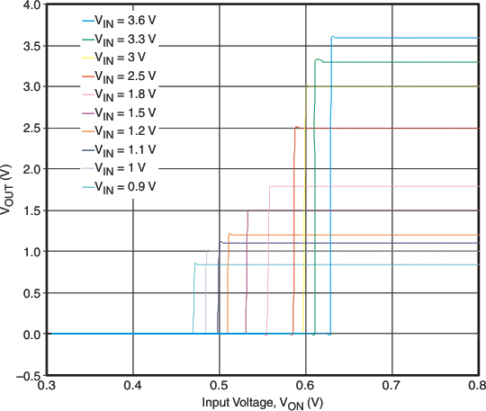 Figure 10. ON-Input Threshold
8.14.2 Typical AC Characteristics (TPS22921)
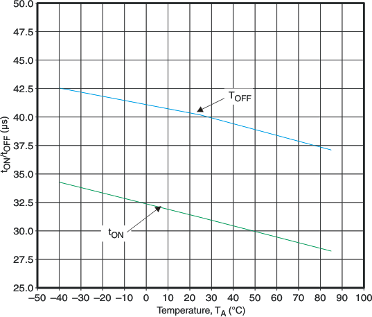 Figure 11. tON/tOFF vs Temperature (VIN = 3.3 V)
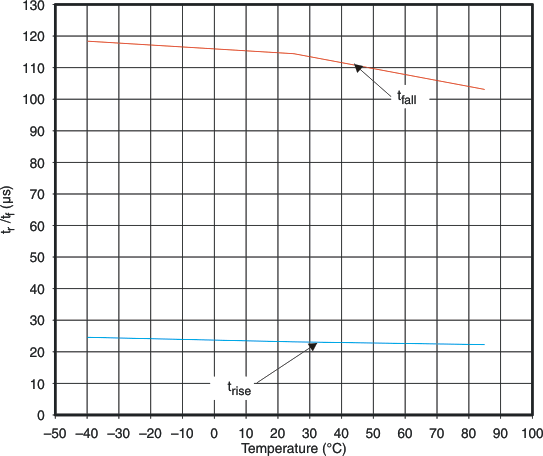 Figure 12. trise/tfall vs Temperature (VIN = 3.3 V)
8.14.3 Typical AC Characteristics (TPS22922)
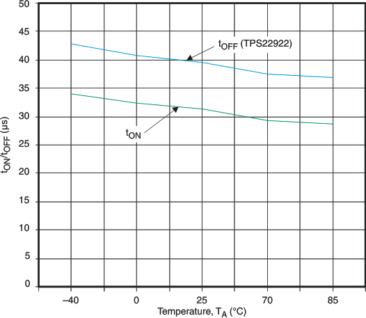 Figure 13. tON/tOFF vs Temperature (VIN = 3.3 V)
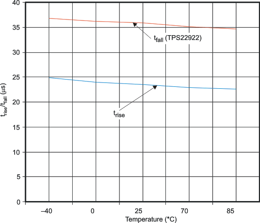 Figure 14. trise/tfall vs Temperature (VIN = 3.3 V)
8.14.4 Typical AC Characteristics (TPS22922B)
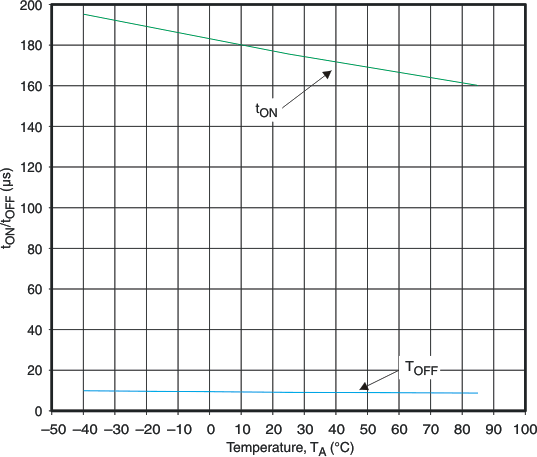 Figure 15. tON/tOFF vs Temperature (VIN = 3.3 V)
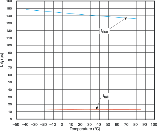 Figure 16. trise/tfall vs Temperature (VIN = 3.3 V)
8.14.5 Typical AC Characteristics (TPS22921 and TPS22922)
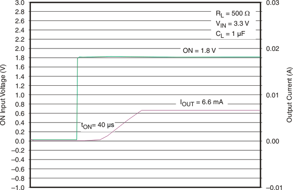 Figure 17. tON Response
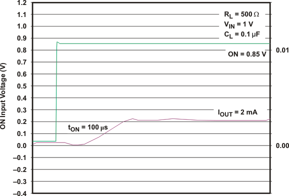 Figure 19. tON Response
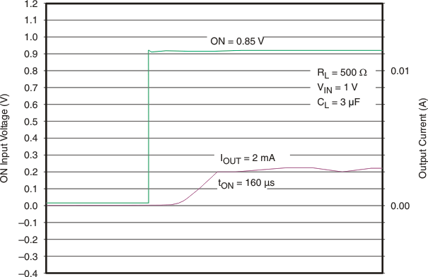 Figure 21. tON Response
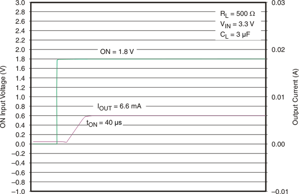 Figure 18. tON Response
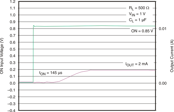 Figure 20. tON Response
8.14.6 Typical AC Characteristics (TPS22921)
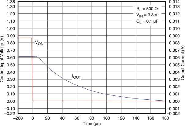 Figure 22. tOFF Response
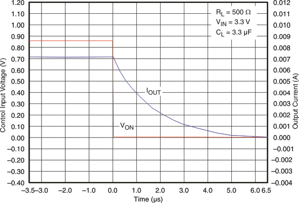 Figure 24. tOFF Response
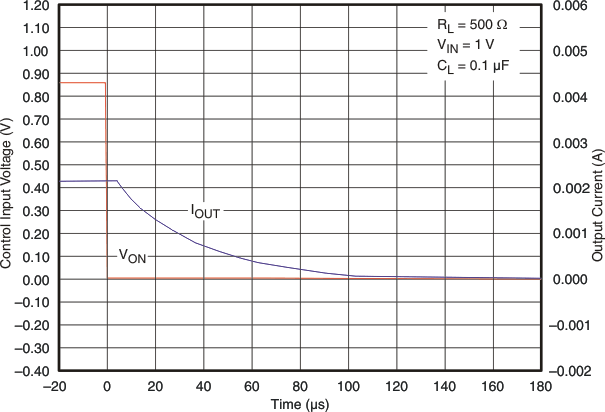 Figure 26. tOFF Response
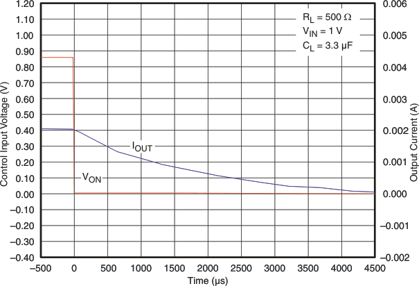 Figure 28. tOFF Response
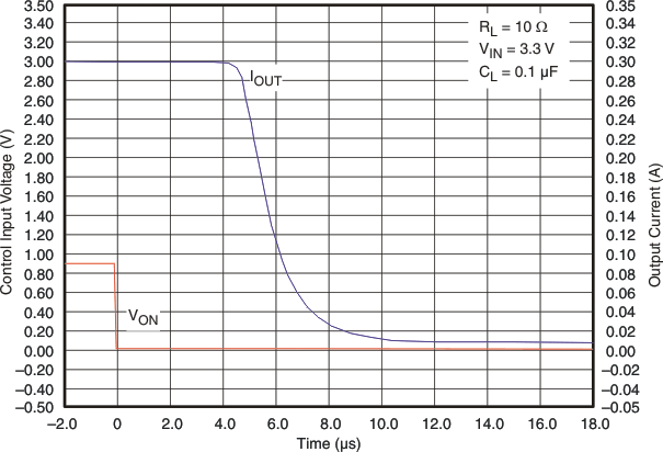 Figure 23. tOFF Response
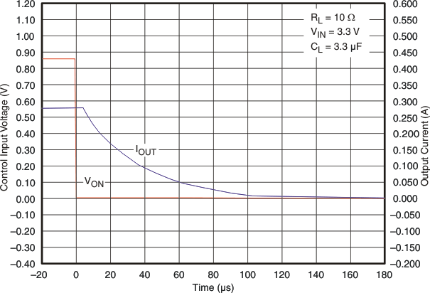 Figure 25. tOFF Response
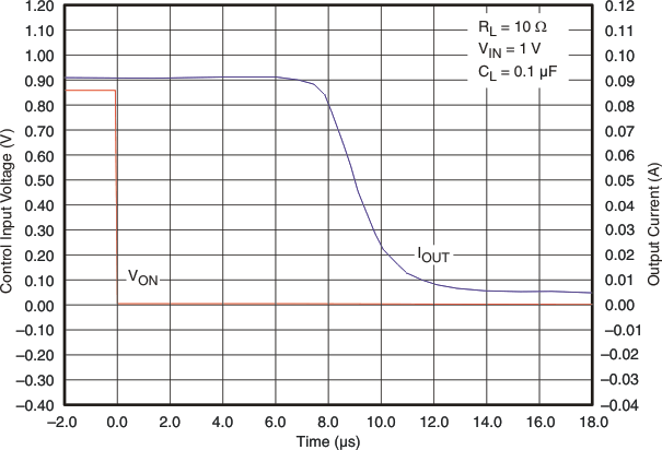 Figure 27. tOFF Response
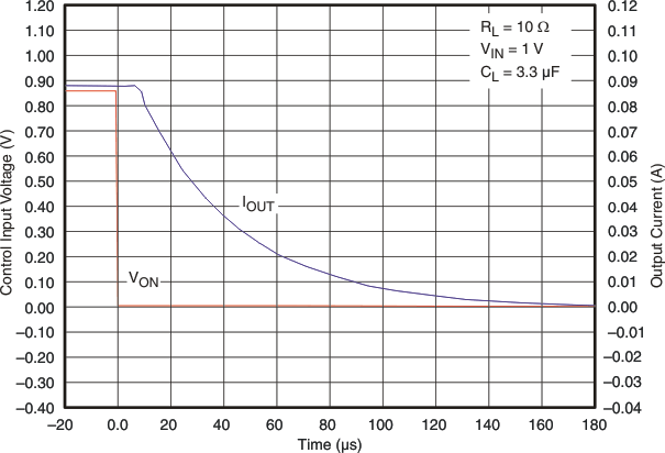 Figure 29. tOFF Response
8.14.7 Typical AC Characteristics (TPS22922)
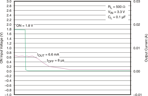 Figure 30. tOFF Response
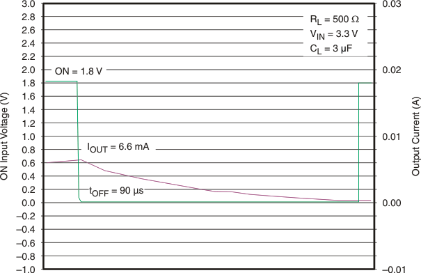 Figure 32. tOFF Response
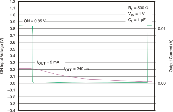 Figure 34. tOFF Response
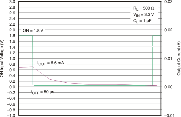 Figure 31. tOFF Response
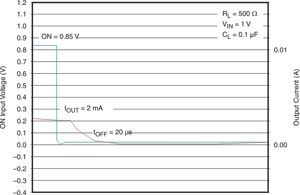 Figure 33. tOFF Response
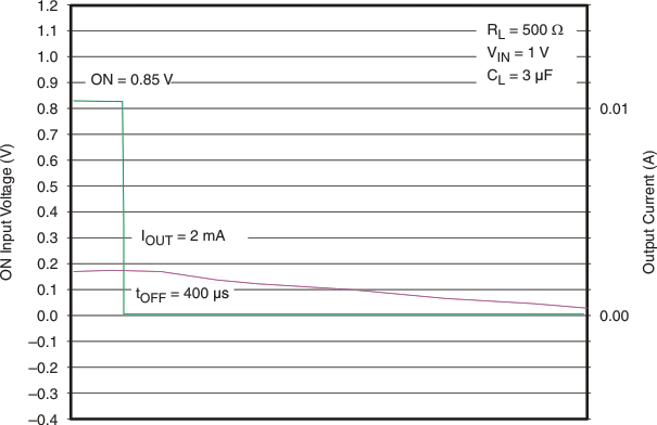 Figure 35. tOFF Response
8.14.8 Typical AC Characteristics (TPS22922B)
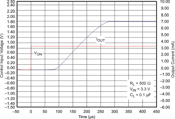 Figure 36. tON Response
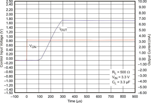 Figure 38. tON Response
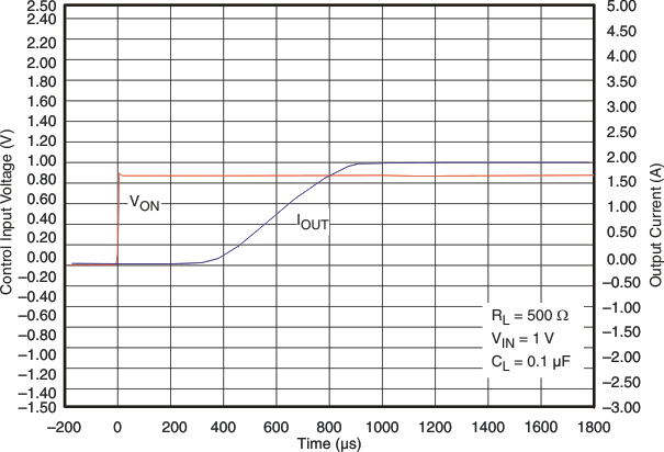 Figure 40. tON Response
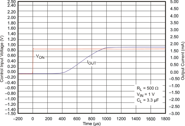 Figure 42. tON Response
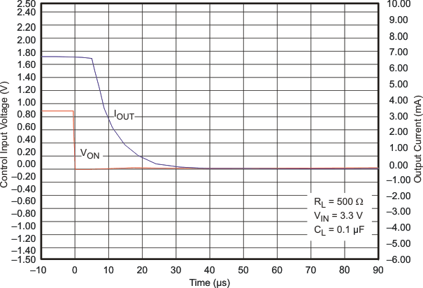 Figure 44. tOFF Response
 Figure 46. tOFF Response
 Figure 48. tOFF Response
 Figure 37. tON Response
 Figure 39. tON Response
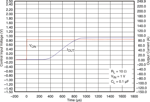 Figure 41. tON Response
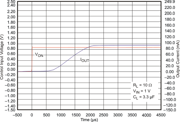 Figure 43. tON Response
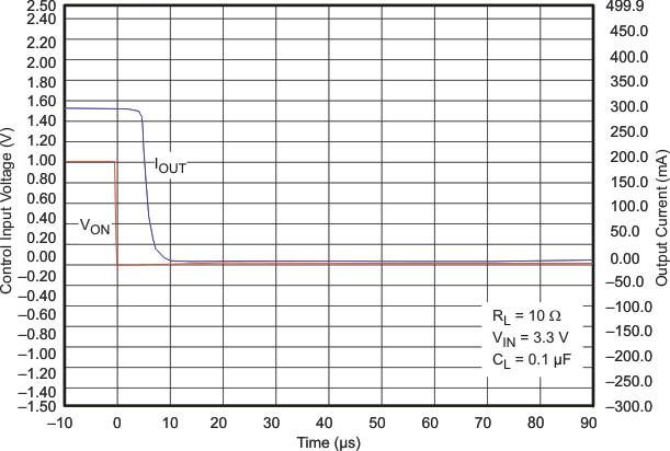 Figure 45. tOFF Response
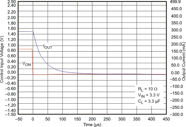 Figure 47. tOFF Response
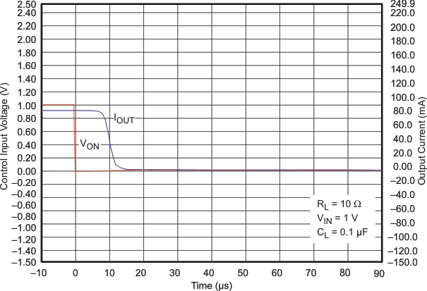 Figure 49. tOFF Response
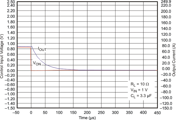 Figure 51. tOFF Response
9 Parameter Measurement Information

10 Detailed Description
10.1 Overview
The TPS2292x is a single-channel, 2-A load switch in a small, space-saving CSP-6 package. These devices implement a P-channel MOSFET to provide a low ON-resistance for a low voltage drop across the device. A controlled rise time is used in applications to limit the inrush current.
10.2 Functional Block Diagram

10.3 Feature Description
10.3.1 ON/OFF Control
The ON pin controls the state of the switch. Activating ON continuously holds the switch in the on state. ON is active high and has a low threshold making it capable of interfacing with low-voltage signals. The ON pin is compatible with standard GPIO logic threshold, and it can be used with any microcontroller with 1.2-V, 1.8-V, 2.5-V or 3.3-V GPIOs.
10.3.2 Quick Output Discharge
The TPS22922 and TPS22922B includes the Quick Output Discharge (QOD) feature. When the switch is disabled, a discharge resistance with a typical value of 65 Ω is connected between the output and ground. This resistance pulls down the output and prevents it from floating when the device is disabled.
10.4 Device Functional Modes
Table 1 lists the VOUT pin connections to for a particular device as determined by the ON pin.
Table 1. VOUT Function Table
| ON | TPS22921 | TPS22922/2B |
|---|---|---|
| L | Open | GND |
| H | VIN | VIN |
11 Application and Implementation
NOTE
Information in the following applications sections is not part of the TI component specification, and TI does not warrant its accuracy or completeness. TI’s customers are responsible for determining suitability of components for their purposes. Customers should validate and test their design implementation to confirm system functionality.
11.1 Application Information
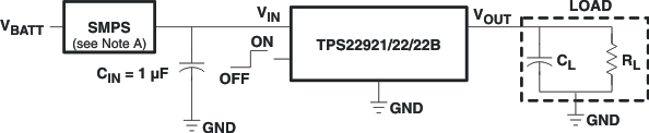
11.1.1 Input Capacitor (Optional)
To limit the voltage drop on the input supply caused by transient inrush currents when the switch turns on into a discharged load capacitor, a capacitor must be placed between VIN and GND. A 1-μF ceramic capacitor, CIN, placed close to the pins is usually sufficient. Higher values of CIN can be used to further reduce the voltage drop during higher current application. When switching a heavy load, TI recommends using an input capacitor about 10 or more times higher than the output capacitor in order to avoid any supply drop.
11.1.2 Output Capacitor (Optional)
Because of the integral body diode in the PMOS switch, a CIN greater than CL is highly recommended. A CL greater than CIN can cause VOUT to exceed VIN when the system supply is removed. This could result in current flow through the body diode from VOUT to VIN.
11.2 Typical Application
11.2.1 Design Requirements
Table 2. Design Parameters
| DESIGN PARAMETER | EXAMPLE VALUE |
|---|---|
| VIN | 1.8 V |
| CL | 4.7 µF |
| Load current | 2 A |
| Ambient Temperature | 25 °C |
| Maximum inrush current | 200 mA |
11.2.2 Detailed Design Procedure
11.2.2.1 Managing Inrush Current
When the switch is enabled, the output capacitors must be charged up from 0 V to the set value (1.8 V in this example). This charge arrives in the form of inrush current. Inrush current can be calculated using the following equation:

where
- CL = Output capacitance
- dVOUT = Output voltage
- dt = Rise time
The TPS22921/2/2B offers a controlled rise time for minimizing inrush current. This device can be selected based upon the minimum acceptable rise time which can be calculated using the design requirements and the inrush current equation. An output capacitance of 4.7 µF will be used because the amount of inrush current increases with output capacitance:
where
- dt = 42.3 µs
To ensure an inrush current of less than 200 mA, a device with a rise time greater than 42.3 µs must be used. The TPS22922B has a typical rise time of 200 µs at 1.8 V which meets the above design requirements. The TPS22921/2 has a faster rise time of 30 µs at 1.8 V, and this would result in an inrush current larger than desired.
11.2.2.2 VIN to VOUT Voltage Drop
The voltage drop from VIN to VOUT is determined by the ON-resistance of the device and the load current. RON can be found in Electrical Characteristics and is dependent on temperature. When the value of RON is found, the following equation can be used to calculate the voltage drop across the device:
where
- ΔV = Voltage drop across the device
- ILOAD = Load current
- RON = ON-resistance of the device
At VIN = 1.8 V, the TPS22921/2/2B has an RON value of 33 mΩ. Using this value and the defined load current, the above equation can be evaluated:
where
- ΔV = 66 mV
Therefore, the voltage drop across the device will be 66 mV.
11.2.3 Application Curve
Figure 54 shows the expected voltage drop across the device for different load currents and input voltages.
Figure 54. Voltage Drop vs Load Current
12 Power Supply Recommendations
The device is designed to operate with a VIN range of 0.9 V to 3.6 V. This supply must be well regulated and placed as close to the device terminals as possible. It must also be able to withstand all transient and load currents, using a recommended input capacitance of 1 µF if necessary. If the supply is located more than a few inches from the device terminals, additional bulk capacitance may be required in addition to the ceramic bypass capacitors. If additional bulk capacitance is required, an electrolytic, tantalum, or ceramic capacitor of 10 µF may be sufficient.