-
TPS65023-Q1 Power Management IC (PMIC) With 3 DC/DCs, 3 LDOs, I2C Interface and DVS
- 1 Features
- 2 Applications
- 3 Description
- 4 Revision History
- 5 Description (continued)
- 6 Pin Configuration and Functions
- 7 Specifications
-
8 Detailed Description
- 8.1 Overview
- 8.2 Functional Block Diagram
- 8.3 Feature Description
- 8.4 Device Functional Modes
- 8.5 Programming
- 8.6
Register Maps
- 8.6.1 VERSION Register (address: 00h) Read-Only
- 8.6.2 PGOODZ Register (address: 01h) Read-Only
- 8.6.3 MASK Register (address: 02h)
- 8.6.4 REG_CTRL Register (address: 03h)
- 8.6.5 CON_CTRL Register (address: 04h)
- 8.6.6 CON_CTRL2 Register (address: 05h)
- 8.6.7 DEFCORE Register (address: 06h)
- 8.6.8 DEFSLEW Register (address: 07h)
- 8.6.9 LDO_CTRL Register (address: 08h)
- 9 Application and Implementation
- 10Power Supply Recommendations
- 11Layout
- 12Device and Documentation Support
- 13Mechanical, Packaging, and Orderable Information
- IMPORTANT NOTICE
DATA SHEET
TPS65023-Q1 Power Management IC (PMIC) With 3 DC/DCs, 3 LDOs, I2C Interface and DVS
1 Features
- Qualified for Automotive Applications
- AEC-Q100 Qualified With the Following Results:
- Device Temperature Grade 1: –40°C to 125°C Ambient Operating Temperature Range
- Device HBM ESD Classification Level 2
- Device CDM ESD Classification Level C4A (RHA Package) or C5 (RSB Package)
- 1.5 A, 90% Efficient Step-Down Converter for Processor Core (VDCDC1)
- 1.2 A, Up to 95% Efficient Step-Down Converter for System Voltage (VDCDC2)
- 1 A, 92% Efficient Step-Down Converter for Memory Voltage (VDCDC3)
- 30 mA LDO/Switch for Real Time Clock (VRTC)
- 2 × 200 mA General-Purpose Low Dropout (LDO)
- Dynamic Voltage Management for Processor Core
- Preselectable LDO Voltage Using Two Digital Input Pins
- Externally Adjustable Reset Delay Time
- Battery Backup Functionality
- Separate Enable Pins for Inductive Converters
- I2C-Compatible Serial Interface
- 85-μA Quiescent Current
- Low-Ripple Pulse-Frequency Modulation (PFM) Mode
- Thermal Shutdown Protection
3 Description
The TPS65023-Q1 device is an integrated power-management integrated circuit (IC) for applications powered by one Li-Ion or Li-Polymer cell, which require multiple power rails. The TPS65023-Q1 device provides three highly efficient, step-down converters targeted at providing the core voltage, peripheral, input and output (I/O), and memory rails in a processor-based system. The core converter allows for on-the-fly voltage changes through a serial interface, allowing the system to implement dynamic power savings. All three step-down converters enter a low-power mode at light load for maximum efficiency across the widest possible range of load currents.
Device Information(1)
| PART NUMBER | PACKAGE | BODY SIZE (NOM) |
|---|---|---|
| TPS65023-Q1 | VQFN (40) | 6.00 mm × 6.00 mm |
| WQFN (40) | 5.00 mm × 5.00 mm |
- For all available packages, see the orderable addendum at the end of the data sheet.
Device Images
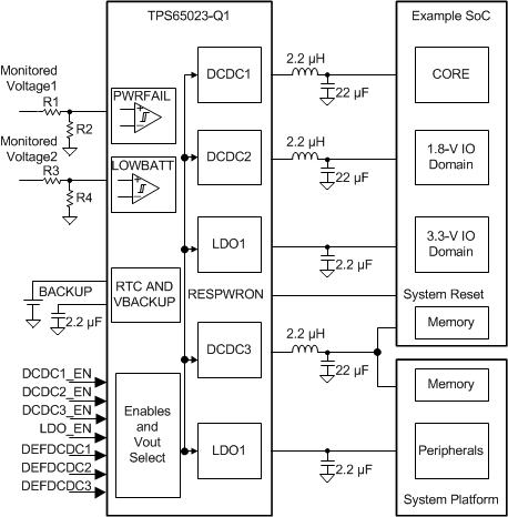
Simplified Schematic
