SLVS927F March 2009 – July 2018 TPS65023-Q1
PRODUCTION DATA.
- 1 Features
- 2 Applications
- 3 Description
- 4 Revision History
- 5 Description (continued)
- 6 Pin Configuration and Functions
- 7 Specifications
-
8 Detailed Description
- 8.1 Overview
- 8.2 Functional Block Diagram
- 8.3 Feature Description
- 8.4 Device Functional Modes
- 8.5 Programming
- 8.6
Register Maps
- 8.6.1 VERSION Register (address: 00h) Read-Only
- 8.6.2 PGOODZ Register (address: 01h) Read-Only
- 8.6.3 MASK Register (address: 02h)
- 8.6.4 REG_CTRL Register (address: 03h)
- 8.6.5 CON_CTRL Register (address: 04h)
- 8.6.6 CON_CTRL2 Register (address: 05h)
- 8.6.7 DEFCORE Register (address: 06h)
- 8.6.8 DEFSLEW Register (address: 07h)
- 8.6.9 LDO_CTRL Register (address: 08h)
- 9 Application and Implementation
- 10Power Supply Recommendations
- 11Layout
- 12Device and Documentation Support
- 13Mechanical, Packaging, and Orderable Information
7.7 Typical Characteristics
Table 1. EVM Parameters for Typical Characteristics Measurement(1)
| CONVERTER | INDUCTOR | OUTPUT CAPACITOR | OUTPUT CAPACITOR VALUE |
|---|---|---|---|
| VDCDC1 | VLCF4020-2R2 | C2012X5R0J106M | 2 × 10 μF |
| VDCDC2 | VLCF4020-2R2 | C2012X5R0J106M | 2 × 10 μF |
| VDCDC3 | VLF4012AT-2R2M1R5 | C2012X5R0J106M | 2 × 10 μF |
(1) Graphs were taken using the evaluation module (EVM), TPS65023EVM-205, with the inductor and output capacitor combinations in Table 1. See TPS65023EVM, User's Guide for more information.
Table 2. Table Of Graphs
| FIGURE | ||
|---|---|---|
| Efficiency | vs Output current | Figure 2, Figure 3, Figure 4, Figure 5, Figure 6, Figure 7 |
| Output voltage | vs Output current at 85°C | Figure 8, Figure 9 |
| Line transient response | Figure 10, Figure 11, Figure 12 | |
| Load transient response | Figure 13, Figure 14, Figure 15 | |
| VDCDC2 PFM operation | Figure 16 | |
| VDCDC2 low ripple PFM operation | Figure 17 | |
| VDCDC2 PWM operation | Figure 18 | |
| Startup VDCDC1, VDCDC2 and VDCDC3 | Figure 19 | |
| Startup LDO1 and LDO2 | Figure 20 | |
| Line transient response | Figure 21, Figure 22, Figure 23 | |
| Load transient response | Figure 24, Figure 25, Figure 26 | |
 Figure 2. DCDC1: Efficiency vs Output Current
  Figure 4. DCDC2: Efficiency vs Output Current
  Figure 6. DCDC3: Efficiency vs Output Current
 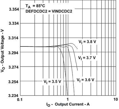 Figure 8. DCDC2: Output Voltage vs Output Current At 85°C
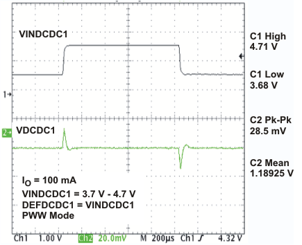
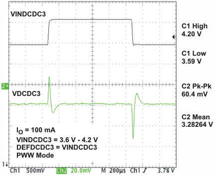 Figure 12. VDCDC3 Line Transient Response
 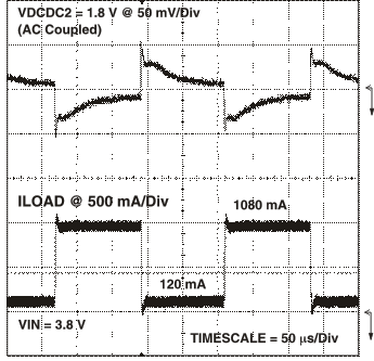 Figure 14. VDCDC2 Load Transient Response
 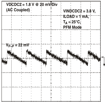 Figure 16. VDCDC2 Output Voltage Ripple
 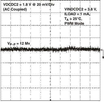 Figure 18. VDCDC2 Output Voltage Ripple
 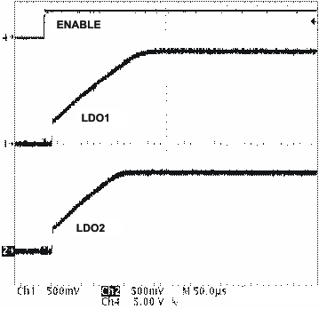 Figure 20. Startup LDO1 and LDO2
 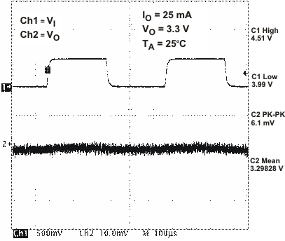 Figure 22. LDO2 Line Transient Response
 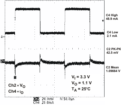 Figure 24. LDO1 Load Transient Response
 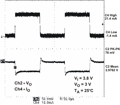 Figure 26. VRTC Load Transient Response
 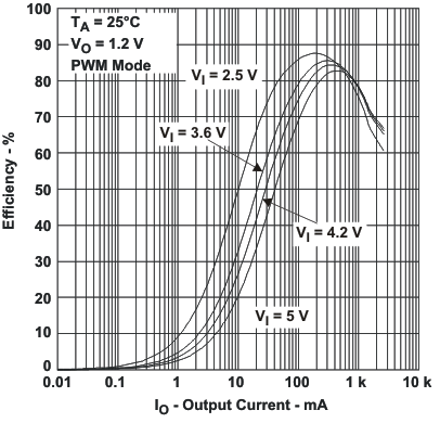 Figure 3. DCDC1: Efficiency vs Output Current
 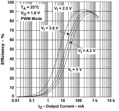 Figure 5. DCDC2: Efficiency vs Output Current
 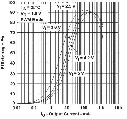 Figure 7. DCDC3: Efficiency vs Output Current
 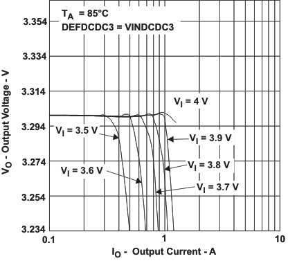 Figure 9. DCDC3: Output Voltage vs Output Current At 85°C
 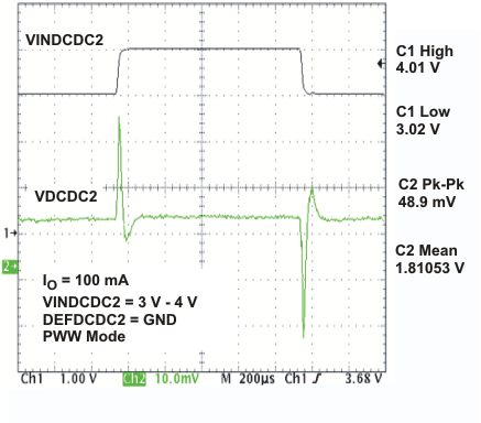 Figure 11. VDCDC2 Line Transient Response
 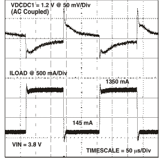 Figure 13. VDCDC1 Load Transient Response
 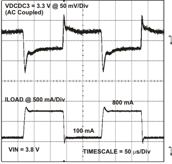 Figure 15. VDCDC3 Load Transient Response
 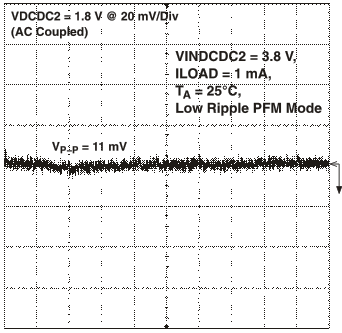 Figure 17. VDCDC2 Output Voltage Ripple
 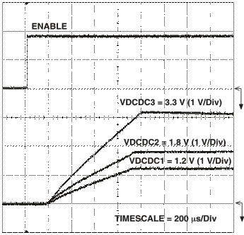 Figure 19. Startup VDCDC1, VDCDC2, and VDCDC3
 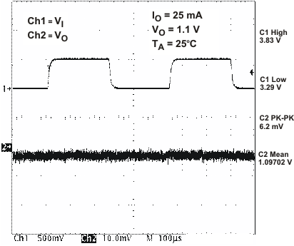 Figure 21. LDO1 Line Transient Response
 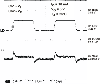 Figure 23. VRTC Line Transient Response
 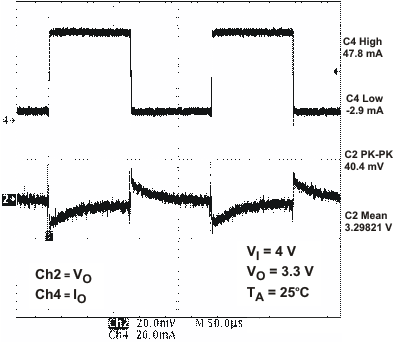 Figure 25. LDO2 Load Transient Response