SLVSAF7C September   2010  – April 2019 TPS61251

PRODUCTION DATA.  

  1. Features
  2. Applications
  3. Description
    1.     Device Images
      1.      Simplified Schematic
  4. Revision History
  5. Description (Continued)
  6. Device Options
  7. Pin Configuration and Functions
    1.     Pin Functions
  8. Specifications
    1. 8.1 Absolute Maximum Ratings
    2. 8.2 ESD Ratings
    3. 8.3 Recommended Operating Conditions
    4. 8.4 Thermal Information
    5. 8.5 Electrical Characteristics
    6. 8.6 Typical Characteristics
  9. Detailed Description
    1. 9.1 Overview
    2. 9.2 Functional Block Diagram
    3. 9.3 Feature Description
      1. 9.3.1 Current Limit Operation
      2. 9.3.2 Soft Start
      3. 9.3.3 Enable
      4. 9.3.4 Undervoltage Lockout (UVLO)
      5. 9.3.5 Power Good
      6. 9.3.6 Input Overvoltage Protection
      7. 9.3.7 Load Disconnect and Reverse Current Protection
      8. 9.3.8 Thermal Regulation
      9. 9.3.9 Thermal Shutdown
    4. 9.4 Device Functional Modes
      1. 9.4.1 Power-Save Mode
      2. 9.4.2 Snooze Mode
      3. 9.4.3 100% Duty-Cycle Mode
  10. 10Application and Implementation
    1. 10.1 Application Information
    2. 10.2 Typical Application
      1. 10.2.1 Design Requirements
      2. 10.2.2 Detailed Design Procedure
        1. 10.2.2.1 Custom Design With WEBENCH® Tools
        2. 10.2.2.2 Output Voltage Setting
        3. 10.2.2.3 Average Input Current Limit
        4. 10.2.2.4 Maximum Output Current
        5. 10.2.2.5 Inductor Selection
        6. 10.2.2.6 Output Capacitor
        7. 10.2.2.7 Input Capacitor
        8. 10.2.2.8 Checking Loop Stability
      3. 10.2.3 Application Curves
  11. 11Power Supply Recommendations
  12. 12Layout
    1. 12.1 Layout Guidelines
    2. 12.2 Layout Example
    3. 12.3 Thermal Consideration
  13. 13Device and Documentation Support
    1. 13.1 Device Support
      1. 13.1.1 Third-Party Products Disclaimer
    2. 13.2 Development Support
      1. 13.2.1 Custom Design With WEBENCH® Tools
    3. 13.3 Receiving Notification of Documentation Updates
    4. 13.4 Community Resource
    5. 13.5 Trademarks
    6. 13.6 Electrostatic Discharge Caution
    7. 13.7 Glossary
  14. 14Mechanical, Packaging, and Orderable Information

Application Curves

Table 4. Table Of Graphs

DESCRIPTION FIGURE
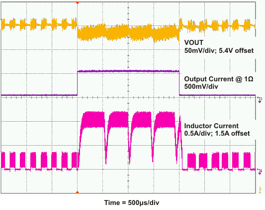
Waveforms Load transient response (Tantal Capacitor 2.3 mF with >60 mΩ ESR, VOUT = 5.5 V, VIN = 3.6 V, ILIM = 1000 mA, Load change from 50 mA to 550 mA) Figure 7
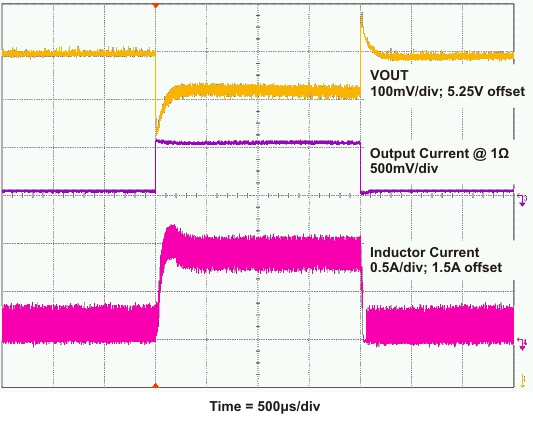
Load transient response (6 × 330-uF Polymer Tantal <5 mΩ ESR in total, VOUT = 5.5 V, VIN = 3.6 V, ILIM = 1000 mA, Load change from 500 mA to 1500 mA) Figure 8
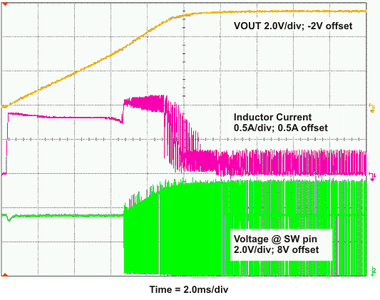
Start-up after enable (VOUT = 5.5 V, VIN = 3.6 V, ILIM = 1000 mA) Figure 9
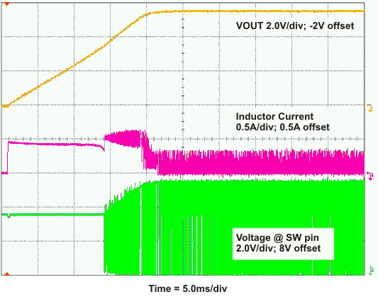
Start-up after enable (VOUT = 5.5 V, VIN = 3.6 V, ILIM = 500 mA) Figure 10

SPACE

TPS61251 meas_trans50to500Ilim1000mAhighESR_lvsaf7.gif
Figure 7. Load Transient Response (Tantal Capacitor)
TPS61251 meas_Startup1000mA_lvsaf7.gif
Figure 9. Start-Up After Enable ILIM = 1000 mA, No Load
TPS61251 meas_trans50to500Ilim1000mAlowESR_lvsaf7.gif
Figure 8. Load Transient Response (Low ESR Polymer Tantal)
TPS61251 meas_Startup500mA_lvsaf7.gif
Figure 10. Start-Up After Enable ILIM = 500 mA, No Load

Table 5 lists the components used for the waveform measurements.

Table 5. List Of Components

REFERENCE DESCRIPTION MANUFACTURER
U1 TPS61251 Texas Instruments
L1 1 μH, 2.1 A, 27 mΩ, 2.8 mm × 2.8 mm × 1.5 mm DEM2815C, TOKO
C1 1 × 4.7 μF, 10 V, 0805, X7R ceramic GRM21BR71A475KA73, Murata
C2 1 × 1000 pF, 50 V, 0603, COG ceramic GRM1885C1H102JA01B, Murata
C3 1 × 4.7 μF, 10 V, 0805, X7R ceramic GRM21BR71A475KA73, Murata
C4 20 × 100 uF, 6.3 V, 1206, X5R GRM31CR60J107ME39B, Murata
R1 Depending on the output voltage of TPS61251, 1% (all waveform measurements with 5.5 V output voltage uses 1000 kΩ)
R2 Depending on the output voltage of TPS61251, 1% (all waveform measurements with 5 V output voltage uses 280 kΩ)
R3 Depending on the input current limit of TPS61251, 1%
R4 1 MΩ, 1% any