SLVSAF7C September   2010  – April 2019 TPS61251

PRODUCTION DATA.  

  1. Features
  2. Applications
  3. Description
    1.     Device Images
      1.      Simplified Schematic
  4. Revision History
  5. Description (Continued)
  6. Device Options
  7. Pin Configuration and Functions
    1.     Pin Functions
  8. Specifications
    1. 8.1 Absolute Maximum Ratings
    2. 8.2 ESD Ratings
    3. 8.3 Recommended Operating Conditions
    4. 8.4 Thermal Information
    5. 8.5 Electrical Characteristics
    6. 8.6 Typical Characteristics
  9. Detailed Description
    1. 9.1 Overview
    2. 9.2 Functional Block Diagram
    3. 9.3 Feature Description
      1. 9.3.1 Current Limit Operation
      2. 9.3.2 Soft Start
      3. 9.3.3 Enable
      4. 9.3.4 Undervoltage Lockout (UVLO)
      5. 9.3.5 Power Good
      6. 9.3.6 Input Overvoltage Protection
      7. 9.3.7 Load Disconnect and Reverse Current Protection
      8. 9.3.8 Thermal Regulation
      9. 9.3.9 Thermal Shutdown
    4. 9.4 Device Functional Modes
      1. 9.4.1 Power-Save Mode
      2. 9.4.2 Snooze Mode
      3. 9.4.3 100% Duty-Cycle Mode
  10. 10Application and Implementation
    1. 10.1 Application Information
    2. 10.2 Typical Application
      1. 10.2.1 Design Requirements
      2. 10.2.2 Detailed Design Procedure
        1. 10.2.2.1 Custom Design With WEBENCH® Tools
        2. 10.2.2.2 Output Voltage Setting
        3. 10.2.2.3 Average Input Current Limit
        4. 10.2.2.4 Maximum Output Current
        5. 10.2.2.5 Inductor Selection
        6. 10.2.2.6 Output Capacitor
        7. 10.2.2.7 Input Capacitor
        8. 10.2.2.8 Checking Loop Stability
      3. 10.2.3 Application Curves
  11. 11Power Supply Recommendations
  12. 12Layout
    1. 12.1 Layout Guidelines
    2. 12.2 Layout Example
    3. 12.3 Thermal Consideration
  13. 13Device and Documentation Support
    1. 13.1 Device Support
      1. 13.1.1 Third-Party Products Disclaimer
    2. 13.2 Development Support
      1. 13.2.1 Custom Design With WEBENCH® Tools
    3. 13.3 Receiving Notification of Documentation Updates
    4. 13.4 Community Resource
    5. 13.5 Trademarks
    6. 13.6 Electrostatic Discharge Caution
    7. 13.7 Glossary
  14. 14Mechanical, Packaging, and Orderable Information

Typical Characteristics

Table 1. Table Of Graphs

DESCRIPTION FIGURE
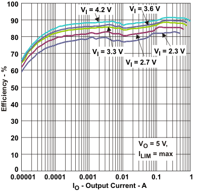
Efficiency vs Output current (VOUT = 5.5 V, ILIM = 1.5 A, R1 = 2320 kΩ and R2 = 649 kΩ) Figure 1
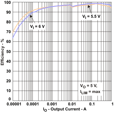
vs Output current in 100% Duty-Cycle Mode (VOUT = 5.5V, ILIM = 1.5 A, R1 = 2320 kΩ and R2 = 649 kΩ) Figure 2
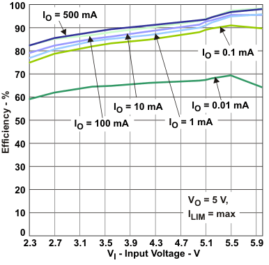
vs Input voltage (VOUT = 5.5 V, ILOAD = {0.01;0.1; 1.0; 10; 100; 500 mA}, R1 = 2320 kΩ and R2 = 649 kΩ) Figure 3
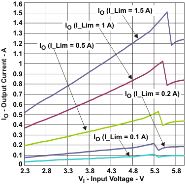
Maximum output current vs Input voltage (VOUT = 5.5 V, ILIM = {100; 200; 500; 1000; 1500 mA}, R1 = 1000 kΩ and R2 = 280 kΩ) Figure 4
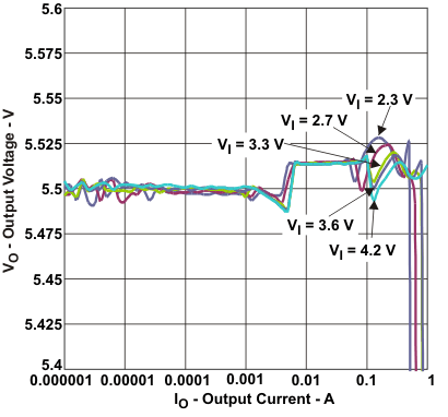
Output voltage vs Output current (VOUT = 5.5 V, ILIM = 1.5 A, R1 = 1000 kΩ and R2 = 280 kΩ) Figure 5
TPS61251 eff1_io_lvsaf7.gif
Figure 1. Efficiency vs Output Current
TPS61251 eff2_vi_lvsaf7.gif
Figure 3. Efficiency vs Input Voltage
TPS61251 vo_io_lvsaf7.gif
Figure 5. Output Voltage vs Output Current
TPS61251 eff3_io100_lvsaf7.gif
Figure 2. Efficiency vs Output Current In 100% Duty-Cycle Mode
TPS61251 max_io_vi_lvsaf7.gif
Figure 4. Maximum Output Current vs Input Voltage